- 您现在的位置:买卖IC网 > PDF目录11949 > PC9RS08KA2PAE (Freescale Semiconductor)MCU 8BIT 2KB FLASH RS08 8-DIP PDF资料下载
参数资料
| 型号: | PC9RS08KA2PAE |
| 厂商: | Freescale Semiconductor |
| 文件页数: | 16/136页 |
| 文件大小: | 0K |
| 描述: | MCU 8BIT 2KB FLASH RS08 8-DIP |
| 标准包装: | 50 |
| 系列: | RS08 |
| 核心处理器: | RS08 |
| 芯体尺寸: | 8-位 |
| 速度: | 10MHz |
| 外围设备: | LVD,POR,WDT |
| 输入/输出数: | 4 |
| 程序存储器容量: | 2KB(2K x 8) |
| 程序存储器类型: | 闪存 |
| RAM 容量: | 63 x 8 |
| 电压 - 电源 (Vcc/Vdd): | 1.8 V ~ 5.5 V |
| 振荡器型: | 内部 |
| 工作温度: | 0°C ~ 70°C |
| 封装/外壳: | 8-DIP(0.300",7.62mm) |
| 包装: | 管件 |
| 配用: | DEMO9RS08KA2-ND - DEMO BOARD FOR 9RS08KA2 |
第1页第2页第3页第4页第5页第6页第7页第8页第9页第10页第11页第12页第13页第14页第15页当前第16页第17页第18页第19页第20页第21页第22页第23页第24页第25页第26页第27页第28页第29页第30页第31页第32页第33页第34页第35页第36页第37页第38页第39页第40页第41页第42页第43页第44页第45页第46页第47页第48页第49页第50页第51页第52页第53页第54页第55页第56页第57页第58页第59页第60页第61页第62页第63页第64页第65页第66页第67页第68页第69页第70页第71页第72页第73页第74页第75页第76页第77页第78页第79页第80页第81页第82页第83页第84页第85页第86页第87页第88页第89页第90页第91页第92页第93页第94页第95页第96页第97页第98页第99页第100页第101页第102页第103页第104页第105页第106页第107页第108页第109页第110页第111页第112页第113页第114页第115页第116页第117页第118页第119页第120页第121页第122页第123页第124页第125页第126页第127页第128页第129页第130页第131页第132页第133页第134页第135页第136页
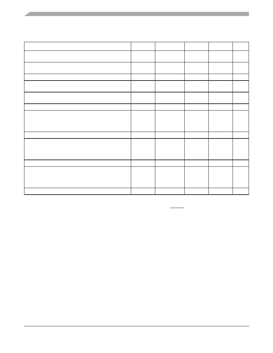
Appendix A Electrical Characteristics
MC9RS08KA2 Series Data Sheet, Rev. 4
112
Freescale Semiconductor
Input low voltage (VDD > 2.3 V) (all digital inputs)
VIL
——
0.30
×
VDD
V
Input low voltage (1.8 V
≤ V
DD ≤ 2.3 V)
(all digital inputs)
VIL
——
0.30
×
VDD
V
Input hysteresis (all digital inputs)
Vhys
0.06
× V
DD
——
V
Input leakage current (per pin)
VIn = VDD or VSS, all input only pins
|IIn|—
0.025
1.0
μA
High impedance (off-state) leakage current (per pin)
VIn = VDD or VSS, all input/output
|IOZ|—
0.025
1.0
μA
Internal pullup/pulldown resistors2 (all port pins)
RPU
20
45
65
k
Ω
Output high voltage (port A)
IOH = –5 mA (VDD ≥ 4.5 V)
IOH = –3 mA (VDD ≥ 3 V)
IOH = –2 mA (VDD ≥ 1.8 V)
VOH
VDD – 0.8
—
V
Maximum total IOH for all port pins
|IOHT|—
—
40
mA
Output low voltage (port A)
IOL = 5 mA (VDD ≥ 4.5 V)
IOL = 3 mA (VDD ≥ 3 V)
IOL = 2 mA (VDD ≥ 1.8 V)
VOL
——
0.8
V
Maximum total IOL for all port pins
IOLT
——
40
mA
dc injection current3, 4, 5 6
VIn < VSS, VIn > VDD
Single pin limit
Total MCU limit, includes sum of all stressed pins
|IIC|—
—
0.2
0.8
mA
Input capacitance (all non-supply pins)
CIn
——
7
pF
1 This parameter is characterized and not tested on each device.
2 Measurement condition for pull resistors: V
In = VSS for pullup and VIn = VDD for pulldown.
3 All functional non-supply pins are internally clamped to V
SS and VDD except the RESET/VPP which is internally clamped to
VSS only.
4 Input must be current limited to the value specified. To determine the value of the required current-limiting resistor, calculate
resistance values for positive and negative clamp voltages, then use the larger of the two values.
5 Power supply must maintain regulation within operating V
DD range during instantaneous and operating maximum current
conditions. If positive injection current (VIn > VDD) is greater than IDD, the injection current may flow out of VDD and could result
in external power supply going out of regulation. Ensure external VDD load will shunt current greater than maximum injection
current. This will be the greatest risk when the MCU is not consuming power. Examples are: if no system clock is present, or
if clock rate is very low which would reduce overall power consumption.
6 This parameter is characterized and not tested on each device.
Table A-4. DC Characteristics (continued)
(Temperature Range = –40 to 85
°C Ambient)
Parameter
Symbol
Min
Typical
Max
Unit
相关PDF资料 |
PDF描述 |
|---|---|
| PC9RS08KA2FPE | MCU 8BIT 2KB FLASH RS08 6-VDFN |
| PC9RS08KA2DWE | MCU 8BIT 2KB FLASH RS08 8-SOIC |
| VI-B6Z-IX-F1 | CONVERTER MOD DC/DC 2V 30W |
| MPC565MZP56R2 | IC MPU 1M FLASH 56MHZ 388-PBGA |
| MPC565CZP40R2 | IC MPU 1M FLASH 40MHZ 388-PBGA |
相关代理商/技术参数 |
参数描述 |
|---|---|
| PC9RS08KA8CWJ | 制造商:Freescale Semiconductor 功能描述: |
| PC9RS08LA8CFT | 功能描述:8位微控制器 -MCU 8-BIT 8K FLASH W/LCD RoHS:否 制造商:Silicon Labs 核心:8051 处理器系列:C8051F39x 数据总线宽度:8 bit 最大时钟频率:50 MHz 程序存储器大小:16 KB 数据 RAM 大小:1 KB 片上 ADC:Yes 工作电源电压:1.8 V to 3.6 V 工作温度范围:- 40 C to + 105 C 封装 / 箱体:QFN-20 安装风格:SMD/SMT |
| PC9RS08LA8CLF | 功能描述:8位微控制器 -MCU 8-BIT 8K FLASH W/LCD RoHS:否 制造商:Silicon Labs 核心:8051 处理器系列:C8051F39x 数据总线宽度:8 bit 最大时钟频率:50 MHz 程序存储器大小:16 KB 数据 RAM 大小:1 KB 片上 ADC:Yes 工作电源电压:1.8 V to 3.6 V 工作温度范围:- 40 C to + 105 C 封装 / 箱体:QFN-20 安装风格:SMD/SMT |
| PC9RS08LE4CWL | 功能描述:8位微控制器 -MCU 8-BIT 4K FLASH W/LCD RoHS:否 制造商:Silicon Labs 核心:8051 处理器系列:C8051F39x 数据总线宽度:8 bit 最大时钟频率:50 MHz 程序存储器大小:16 KB 数据 RAM 大小:1 KB 片上 ADC:Yes 工作电源电压:1.8 V to 3.6 V 工作温度范围:- 40 C to + 105 C 封装 / 箱体:QFN-20 安装风格:SMD/SMT |
| PC9S08AC128CFGE | 功能描述:8位微控制器 -MCU 8-Bit MCU 128K FLASH 8K RAM RoHS:否 制造商:Silicon Labs 核心:8051 处理器系列:C8051F39x 数据总线宽度:8 bit 最大时钟频率:50 MHz 程序存储器大小:16 KB 数据 RAM 大小:1 KB 片上 ADC:Yes 工作电源电压:1.8 V to 3.6 V 工作温度范围:- 40 C to + 105 C 封装 / 箱体:QFN-20 安装风格:SMD/SMT |
发布紧急采购,3分钟左右您将得到回复。