- 您现在的位置:买卖IC网 > PDF目录11597 > PIC12C508AT-04/SN (Microchip Technology)IC MCU OTP 512X12 8SOIC PDF资料下载
参数资料
| 型号: | PIC12C508AT-04/SN |
| 厂商: | Microchip Technology |
| 文件页数: | 28/113页 |
| 文件大小: | 0K |
| 描述: | IC MCU OTP 512X12 8SOIC |
| 产品培训模块: | Asynchronous Stimulus |
| 标准包装: | 3,300 |
| 系列: | PIC® 12C |
| 核心处理器: | PIC |
| 芯体尺寸: | 8-位 |
| 速度: | 4MHz |
| 外围设备: | POR,WDT |
| 输入/输出数: | 5 |
| 程序存储器容量: | 768B(512 x 12) |
| 程序存储器类型: | OTP |
| RAM 容量: | 25 x 8 |
| 电压 - 电源 (Vcc/Vdd): | 3 V ~ 5.5 V |
| 振荡器型: | 内部 |
| 工作温度: | 0°C ~ 70°C |
| 封装/外壳: | 8-SOIC(0.154",3.90mm 宽) |
| 包装: | 带卷 (TR) |
| 配用: | 309-1046-ND - ADAPTER 8-SOIC TO 8-DIP 309-1045-ND - ADAPTER 8-SOIC TO 8-DIP AC124001-ND - MODULE SKT PROMATEII 8DIP/SOIC |
第1页第2页第3页第4页第5页第6页第7页第8页第9页第10页第11页第12页第13页第14页第15页第16页第17页第18页第19页第20页第21页第22页第23页第24页第25页第26页第27页当前第28页第29页第30页第31页第32页第33页第34页第35页第36页第37页第38页第39页第40页第41页第42页第43页第44页第45页第46页第47页第48页第49页第50页第51页第52页第53页第54页第55页第56页第57页第58页第59页第60页第61页第62页第63页第64页第65页第66页第67页第68页第69页第70页第71页第72页第73页第74页第75页第76页第77页第78页第79页第80页第81页第82页第83页第84页第85页第86页第87页第88页第89页第90页第91页第92页第93页第94页第95页第96页第97页第98页第99页第100页第101页第102页第103页第104页第105页第106页第107页第108页第109页第110页第111页第112页第113页
1999 Microchip Technology Inc.
DS40139E-page 21
PIC12C5XX
5.0
I/O PORT
As with any other register, the I/O register can be
written and read under program control. However, read
instructions (e.g., MOVF GPIO,W) always read the I/O
pins independent of the pin’s input/output modes. On
RESET, all I/O ports are defined as input (inputs are at
hi-impedance) since the I/O control registers are all
set. See Section 7.0 for SCL and SDA description for
PIC12CE5XX.
5.1
GPIO
GPIO is an 8-bit I/O register. Only the low order 6 bits
are used (GP5:GP0). Bits 7 and 6 are unimplemented
and read as '0's. Please note that GP3 is an input only
pin. The configuration word can set several I/O’s to
alternate functions. When acting as alternate functions
the pins will read as ‘0’ during port read. Pins GP0,
GP1, and GP3 can be configured with weak pull-ups
and also with wake-up on change. The wake-up on
change and weak pull-up functions are not pin
selectable. If pin 4 is configured as MCLR, weak pull-
up is always on and wake-up on change for this pin is
not enabled.
5.2
TRIS Register
The output driver control register is loaded with the
contents of the W register by executing the TRIS f
instruction. A '1' from a TRIS register bit puts the
corresponding output driver in a hi-impedance mode.
A '0' puts the contents of the output data latch on the
selected
pins,
enabling
the
output
buffer.
The
exceptions are GP3 which is input only and GP2 which
may be controlled by the option register, see Figure 4-
The TRIS registers are “write-only” and are set (output
drivers disabled) upon RESET.
Note:
A read of the ports reads the pins, not the
output data latches. That is, if an output
driver on a pin is enabled and driven high,
but the external system is holding it low, a
read of the port will indicate that the pin is
low.
5.3
I/O Interfacing
The equivalent circuit for an I/O port pin is shown in
Figure 5-1. All port pins, except GP3 which is input
only, may be used for both input and output operations.
For input operations these ports are non-latching. Any
input must be present until read by an input instruction
(e.g., MOVF
GPIO,W
). The outputs are latched and
remain unchanged until the output latch is rewritten. To
use a port pin as output, the corresponding direction
control bit in TRIS must be cleared (= 0). For use as an
input, the corresponding TRIS bit must be set. Any I/O
pin (except GP3) can be programmed individually as
input or output.
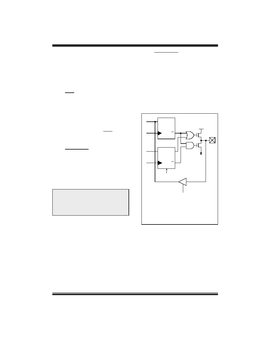
FIGURE 5-1:
EQUIVALENT CIRCUIT
FOR A SINGLE I/O PIN
Data
Bus
Q
D
Q
CK
Q
D
Q
CK
P
N
WR
Port
TRIS ‘f’
Data
TRIS
RD Port
VSS
VDD
I/O
pin(1,3)
W
Reg
Latch
Reset
(2)
Note 1: I/O pins have protection diodes to VDD
and VSS.
Note 2: See Table 3-1 for buffer type.
Note 3: See Section 7.0 for SCL and SDA
description for PIC12CE5XX
相关PDF资料 |
PDF描述 |
|---|---|
| GRM2165C2A162JA01D | CAP CER 1600PF 100V 5% NP0 0805 |
| GRM2165C2A152JA01D | CAP CER 1500PF 100V 5% NP0 0805 |
| GRM2165C2A132JA01D | CAP CER 1300PF 100V 5% NP0 0805 |
| GRM2165C2A122JA01D | CAP CER 1200PF 100V 5% NP0 0805 |
| GRM2165C2A112JA01D | CAP CER 1100PF 100V 5% NP0 0805 |
相关代理商/技术参数 |
参数描述 |
|---|---|
| PIC12C508T | 制造商:MICROCHIP 制造商全称:Microchip Technology 功能描述:8-Pin, 8-Bit CMOS Microcontroller |
| PIC12C508T-04/EJW | 制造商:MICROCHIP 制造商全称:Microchip Technology 功能描述:8-Pin, 8-Bit CMOS Microcontrollers |
| PIC12C508T-04/EP | 制造商:MICROCHIP 制造商全称:Microchip Technology 功能描述:8-Pin, 8-Bit CMOS Microcontrollers |
| PIC12C508T-04/ESM | 制造商:MICROCHIP 制造商全称:Microchip Technology 功能描述:8-Pin, 8-Bit CMOS Microcontrollers |
| PIC12C508T-04/ESN | 制造商:MICROCHIP 制造商全称:Microchip Technology 功能描述:8-Pin, 8-Bit CMOS Microcontrollers |
发布紧急采购,3分钟左右您将得到回复。