- 您现在的位置:买卖IC网 > PDF目录299771 > PIC16C923T-04I/PT 8-BIT, OTPROM, 4 MHz, RISC MICROCONTROLLER, PQFP64 PDF资料下载
参数资料
| 型号: | PIC16C923T-04I/PT |
| 元件分类: | 微控制器/微处理器 |
| 英文描述: | 8-BIT, OTPROM, 4 MHz, RISC MICROCONTROLLER, PQFP64 |
| 封装: | 10 X 10 MM, 1 MM HEIGHT, PLASTIC, TQFP-64 |
| 文件页数: | 152/189页 |
| 文件大小: | 1201K |
| 代理商: | PIC16C923T-04I/PT |
第1页第2页第3页第4页第5页第6页第7页第8页第9页第10页第11页第12页第13页第14页第15页第16页第17页第18页第19页第20页第21页第22页第23页第24页第25页第26页第27页第28页第29页第30页第31页第32页第33页第34页第35页第36页第37页第38页第39页第40页第41页第42页第43页第44页第45页第46页第47页第48页第49页第50页第51页第52页第53页第54页第55页第56页第57页第58页第59页第60页第61页第62页第63页第64页第65页第66页第67页第68页第69页第70页第71页第72页第73页第74页第75页第76页第77页第78页第79页第80页第81页第82页第83页第84页第85页第86页第87页第88页第89页第90页第91页第92页第93页第94页第95页第96页第97页第98页第99页第100页第101页第102页第103页第104页第105页第106页第107页第108页第109页第110页第111页第112页第113页第114页第115页第116页第117页第118页第119页第120页第121页第122页第123页第124页第125页第126页第127页第128页第129页第130页第131页第132页第133页第134页第135页第136页第137页第138页第139页第140页第141页第142页第143页第144页第145页第146页第147页第148页第149页第150页第151页当前第152页第153页第154页第155页第156页第157页第158页第159页第160页第161页第162页第163页第164页第165页第166页第167页第168页第169页第170页第171页第172页第173页第174页第175页第176页第177页第178页第179页第180页第181页第182页第183页第184页第185页第186页第187页第188页第189页
1997 Microchip Technology Inc.
DS30444E - page 65
PIC16C9XX
11.1
SPI Mode
The SPI mode allows 8-bits of data to be synchro-
nously transmitted and received simultaneously. To
accomplish communication, typically three pins are
used:
Serial Data Out (SDO) RC5/SDO
Serial Data In (SDI) RC4/SDI
Serial Clock (SCK) RC3/SCK
Additionally a fourth pin may be used when in a slave
mode of operation:
Slave Select (SS) RA5/AN4/SS (the AN4 function
is implemented on the PIC16C924 only)
When initializing the SPI, several options need to be
specied. This is done by programming the appropriate
control bits in the SSPCON register (SSPCON<5:0>)
and SSPSTAT<7:6>. These control bits allow the fol-
lowing to be specied:
Master Mode (SCK is the clock output)
Slave Mode (SCK is the clock input)
Clock Polarity (Idle state of SCK)
Clock edge (output data on rising/falling edge of
SCK)
Clock Rate (Master mode only)
Slave Select Mode (Slave mode only)
The SSP consists of a transmit/receive Shift Register
(SSPSR) and a buffer register (SSPBUF). The SSPSR
shifts the data in and out of the device, MSb rst. The
SSPBUF holds the data that was written to the SSPSR,
until the received data is ready. Once the 8-bits of data
have been received, that byte is moved to the SSPBUF
register.
Then
the
buffer
full
detect
bit
BF
(SSPSTAT<0>) and interrupt ag bit SSPIF (PIR1<3>)
are set. This double buffering of the received data
(SSPBUF) allows the next byte to start reception before
reading the data that was just received. Any write to the
SSPBUF register during transmission/reception of data
will be ignored, and the write collision detect bit WCOL
(SSPCON<7>) will be set. User software must clear the
WCOL bit so that it can be determined if the following
write(s) to the SSPBUF register completed success-
fully. When the application software is expecting to
receive valid data, the SSPBUF should be read before
the next byte of data to transfer is written to the
SSPBUF. Buffer full bit BF (SSPSTAT<0>) indicates
when SSPBUF has been loaded with the received data
(transmission is complete). When the SSPBUF is read,
bit BF is cleared. This data may be irrelevant if the SPI
is only a transmitter. Generally the SSP Interrupt is
used to determine when the transmission/reception
has completed. The SSPBUF must be read and/or writ-
ten. If the interrupt method is not going to be used, then
software polling can be done to ensure that a write col-
lision does not occur. Example 11-1 shows the loading
of the SSPBUF (SSPSR) for data transmission. The
shaded instruction is only required if the received data
is meaningful.
EXAMPLE 11-1: LOADING THE SSPBUF
(SSPSR) REGISTER
BCF
STATUS, RP1
;Select Bank1
BSF
STATUS, RP0
;
LOOP BTFSS SSPSTAT, BF
;Has data been
;received
;(transmit
;complete)?
GOTO
LOOP
;No
BCF
STATUS, RP0
;Select Bank0
MOVF
SSPBUF, W
;W reg = contents
; of SSPBUF
MOVF
TXDATA, W
;W reg = contents
; of TXDATA
MOVWF SSPBUF
;New data to xmit
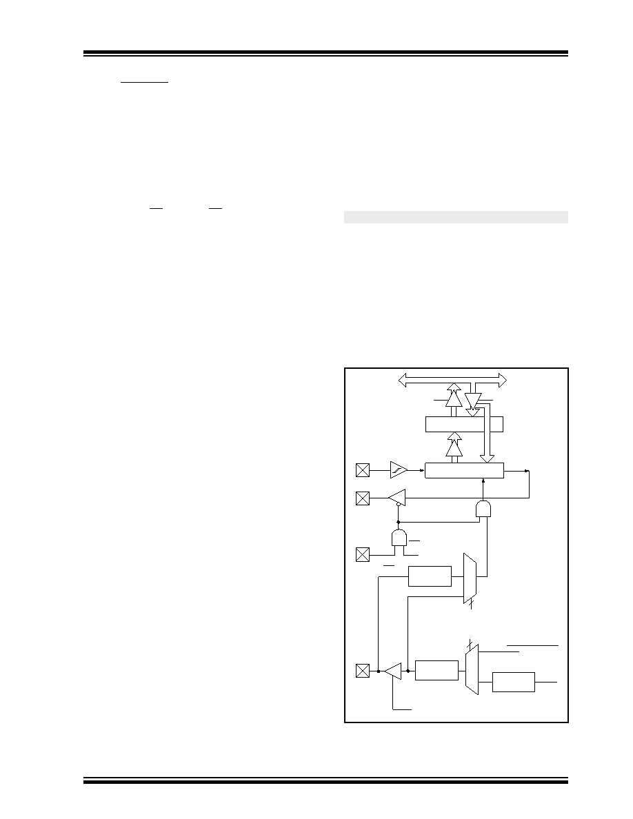
The block diagram of the SSP module, when in SPI
mode (Figure 11-3), shows that the SSPSR is not
directly readable or writable, and can only be accessed
from addressing the SSPBUF register. Additionally, the
SSP status register (SSPSTAT) indicates the various
status conditions.
FIGURE 11-3: SSP BLOCK DIAGRAM
(SPI MODE)
MOVWF RXDATA
;Save in user RAM
Read
Write
Internal
data bus
RC4/SDI/SDA
RC5/SDO
RA5/AN4/SS
RC3/SCK/
SSPSR reg
SSPBUF reg
SSPM3:SSPM0
bit0
shift
clock
SS Control
Enable
Edge
Select
Clock Select
TMR2 output
TCY
Prescaler
4, 16, 64
TRISC<3>
2
Edge
Select
2
4
SCL
相关PDF资料 |
PDF描述 |
|---|---|
| PIC16C925/L | 8-BIT, OTPROM, 20 MHz, RISC MICROCONTROLLER, PQCC68 |
| PIC16C925/PT | 8-BIT, OTPROM, 20 MHz, RISC MICROCONTROLLER, PQFP64 |
| PIC16LC926-I/PT | 8-BIT, OTPROM, 10 MHz, RISC MICROCONTROLLER, PQFP64 |
| PIC16F1518-I/SO | 8-BIT, FLASH, RISC MICROCONTROLLER, PDSO28 |
| PIC16F1518T-E/MV | RISC MICROCONTROLLER, PQCC28 |
相关代理商/技术参数 |
参数描述 |
|---|---|
| PIC16C923T-08/L | 功能描述:8位微控制器 -MCU 7KB 176 RAM 52 I/O RoHS:否 制造商:Silicon Labs 核心:8051 处理器系列:C8051F39x 数据总线宽度:8 bit 最大时钟频率:50 MHz 程序存储器大小:16 KB 数据 RAM 大小:1 KB 片上 ADC:Yes 工作电源电压:1.8 V to 3.6 V 工作温度范围:- 40 C to + 105 C 封装 / 箱体:QFN-20 安装风格:SMD/SMT |
| PIC16C923T-08/PT | 功能描述:8位微控制器 -MCU 7KB 176 RAM 52 I/O RoHS:否 制造商:Silicon Labs 核心:8051 处理器系列:C8051F39x 数据总线宽度:8 bit 最大时钟频率:50 MHz 程序存储器大小:16 KB 数据 RAM 大小:1 KB 片上 ADC:Yes 工作电源电压:1.8 V to 3.6 V 工作温度范围:- 40 C to + 105 C 封装 / 箱体:QFN-20 安装风格:SMD/SMT |
| PIC16C923T-08I/L | 功能描述:8位微控制器 -MCU 7KB 176 RAM 52 I/O RoHS:否 制造商:Silicon Labs 核心:8051 处理器系列:C8051F39x 数据总线宽度:8 bit 最大时钟频率:50 MHz 程序存储器大小:16 KB 数据 RAM 大小:1 KB 片上 ADC:Yes 工作电源电压:1.8 V to 3.6 V 工作温度范围:- 40 C to + 105 C 封装 / 箱体:QFN-20 安装风格:SMD/SMT |
| PIC16C923T-08I/PT | 功能描述:8位微控制器 -MCU 7KB 176 RAM 52 I/O RoHS:否 制造商:Silicon Labs 核心:8051 处理器系列:C8051F39x 数据总线宽度:8 bit 最大时钟频率:50 MHz 程序存储器大小:16 KB 数据 RAM 大小:1 KB 片上 ADC:Yes 工作电源电压:1.8 V to 3.6 V 工作温度范围:- 40 C to + 105 C 封装 / 箱体:QFN-20 安装风格:SMD/SMT |
| PIC16C924/CL | 功能描述:8位微控制器 -MCU 7KB 176 RAM 52 I/O RoHS:否 制造商:Silicon Labs 核心:8051 处理器系列:C8051F39x 数据总线宽度:8 bit 最大时钟频率:50 MHz 程序存储器大小:16 KB 数据 RAM 大小:1 KB 片上 ADC:Yes 工作电源电压:1.8 V to 3.6 V 工作温度范围:- 40 C to + 105 C 封装 / 箱体:QFN-20 安装风格:SMD/SMT |
发布紧急采购,3分钟左右您将得到回复。