- 您现在的位置:买卖IC网 > PDF目录299771 > PIC16C923T-04I/PT 8-BIT, OTPROM, 4 MHz, RISC MICROCONTROLLER, PQFP64 PDF资料下载
参数资料
| 型号: | PIC16C923T-04I/PT |
| 元件分类: | 微控制器/微处理器 |
| 英文描述: | 8-BIT, OTPROM, 4 MHz, RISC MICROCONTROLLER, PQFP64 |
| 封装: | 10 X 10 MM, 1 MM HEIGHT, PLASTIC, TQFP-64 |
| 文件页数: | 48/189页 |
| 文件大小: | 1201K |
| 代理商: | PIC16C923T-04I/PT |
第1页第2页第3页第4页第5页第6页第7页第8页第9页第10页第11页第12页第13页第14页第15页第16页第17页第18页第19页第20页第21页第22页第23页第24页第25页第26页第27页第28页第29页第30页第31页第32页第33页第34页第35页第36页第37页第38页第39页第40页第41页第42页第43页第44页第45页第46页第47页当前第48页第49页第50页第51页第52页第53页第54页第55页第56页第57页第58页第59页第60页第61页第62页第63页第64页第65页第66页第67页第68页第69页第70页第71页第72页第73页第74页第75页第76页第77页第78页第79页第80页第81页第82页第83页第84页第85页第86页第87页第88页第89页第90页第91页第92页第93页第94页第95页第96页第97页第98页第99页第100页第101页第102页第103页第104页第105页第106页第107页第108页第109页第110页第111页第112页第113页第114页第115页第116页第117页第118页第119页第120页第121页第122页第123页第124页第125页第126页第127页第128页第129页第130页第131页第132页第133页第134页第135页第136页第137页第138页第139页第140页第141页第142页第143页第144页第145页第146页第147页第148页第149页第150页第151页第152页第153页第154页第155页第156页第157页第158页第159页第160页第161页第162页第163页第164页第165页第166页第167页第168页第169页第170页第171页第172页第173页第174页第175页第176页第177页第178页第179页第180页第181页第182页第183页第184页第185页第186页第187页第188页第189页
1997 Microchip Technology Inc.
DS30444E - page 141
PIC16C9XX
17.0
ELECTRICAL CHARACTERISTICS
Absolute Maximum Ratings
Ambient temperature under bias............................................................................................................ .-55C to +125C
Storage temperature .............................................................................................................................. -65C to +150C
Voltage on any pin with respect to VSS (except VDD, MCLR, and RA4).......................................... -0.3V to (VDD + 0.3V)
Voltage on VDD with respect to VSS ......................................................................................................... -0.3V to +7.5V
Voltage on MCLR with respect to VSS............................................................................................................. 0V to +14V
Voltage on RA4 with respect to Vss ................................................................................................................ 0V to +14V
Total power dissipation (Note 1) ................................................................................................................................1.0W
Maximum current out of VSS pin ...........................................................................................................................300 mA
Maximum current into VDD pin ..............................................................................................................................250 mA
Input clamp current, IIK (VI < 0 or VI > VDD)
.....................................................................................................................± 20 mA
Output clamp current, IOK (VO < 0 or VO > VDD)
.............................................................................................................± 20 mA
Maximum output current sunk by any I/O pin .........................................................................................................10 mA
Maximum output current sourced by any I/O pin ...................................................................................................10 mA
Maximum current sunk by all Ports combined ......................................................................................................200 mA
Maximum current sourced by all Ports combined ................................................................................................200 mA
Note 1: Power dissipation is calculated as follows: PDIS = VDD x {IDD -
∑ IOH} + ∑ {(VDD - VOH) x IOH} + ∑(VOl x IOL)
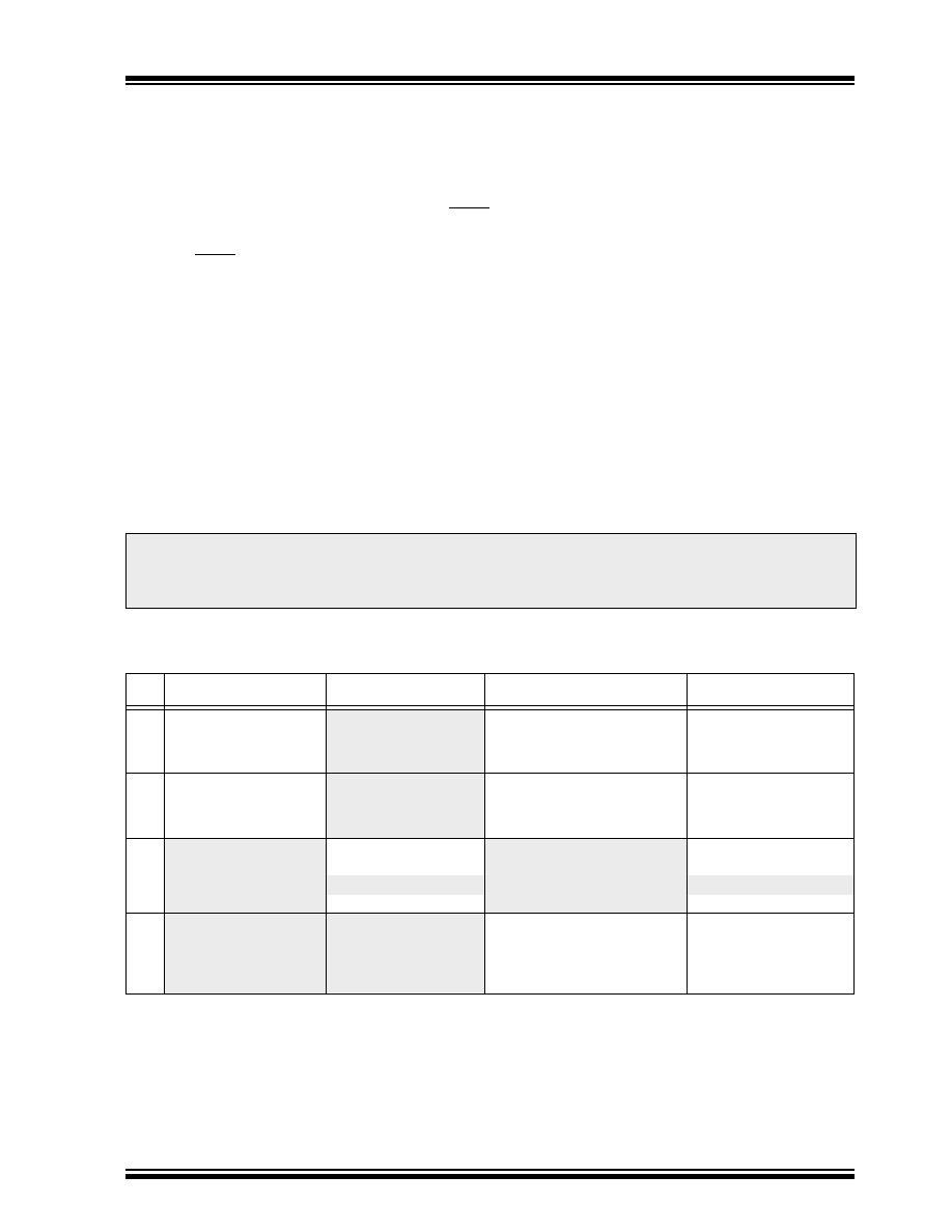
TABLE 17-1: CROSS REFERENCE OF DEVICE SPECS FOR OSCILLATOR CONFIGURATIONS AND
FREQUENCIES OF OPERATION (COMMERCIAL DEVICES)
NOTICE: Stresses above those listed under “Absolute Maximum Ratings” may cause permanent damage to the
device. This is a stress rating only and functional operation of the device at those or any other conditions above those
indicated in the operation listings of this specication is not implied. Exposure to maximum rating conditions for
extended periods may affect device reliability.
OSC
PIC16C923-04
PIC16C924-04
PIC16C923-08
PIC16C924-08
PIC16LC923-04
PIC16LC924-04
CL Devices
RC
VDD: 4.0V to 6.0V
IDD:
5 mA max. at 5.5V
IPD:
21
A max. at 4V
Freq: 4 MHz max.
VDD: 4.5V to 5.5V
IDD:
2.7 mA typ. at 5.5V
IPD:
1.5
A typ. at 4V
Freq: 4 MHz max.
VDD: 2.5V to 6.0V
IDD:
3.8 mA max. at 3.0V
IPD:
5
A max. at 3V
Freq: 4 MHz max.
VDD: 2.5V to 6.0V
IDD:
5 mA max. at 5.5V
IPD:
21
A max. at 4V
Freq: 4 MHz max.
XT
VDD: 4.0V to 6.0V
IDD:
5 mA max. at 5.5V
IPD:
21
A max. at 4V
Freq: 4 MHz max.
VDD: 4.5V to 5.5V
IDD:
2.7 mA typ. at 5.5V
IPD:
1.5
A typ. at 4V
Freq: 4 MHz max.
VDD: 2.5V to 6.0V
IDD:
3.8 mA max. at 3.0V
IPD:
5
A max. at 3V
Freq: 4 MHz max.
VDD: 2.5V to 6.0V
IDD:
5 mA max. at 5.5V
IPD:
21
A max. at 4V
Freq: 4 MHz max.
HS
VDD: 4.5V to 5.5V
Do not use in HS mode
VDD: 4.5V to 5.5V
IDD:
3.5 mA typ. at 5.5V
IDD:
7 mA max. at 5.5V
IDD:
7 mA max. at 5.5V
IPD:
1.5
A typ. at 4.5V
IPD:
1.5
A typ. at 4.5V
IPD:
1.5
A typ. at 4.5V
Freq: 4 MHz max.
Freq: 8 MHz max.
LP
VDD: 4.0V to 6.0V
IDD:
22.5
A typ.
at 32 kHz, 4.0V
IPD:
1.5
A typ. at 4.0V
Freq: 200 kHz max.
Do not use in LP mode
VDD: 2.5V to 6.0V
IDD:
30
A max. at 32 kHz, 3.0V
IPD:
5
A max. at 3.0V
Freq: 200 kHz max.
VDD: 2.5V to 6.0V
IDD:
30
A max.
at 32 kHz, 3.0V
IPD:
5
A max. at 3.0V
Freq: 200 kHz max.
The shaded sections indicate oscillator selections which are tested for functionality, but not for MIN/MAX specications.
It is recommended that the user select the device type that ensures the specications required.
相关PDF资料 |
PDF描述 |
|---|---|
| PIC16C925/L | 8-BIT, OTPROM, 20 MHz, RISC MICROCONTROLLER, PQCC68 |
| PIC16C925/PT | 8-BIT, OTPROM, 20 MHz, RISC MICROCONTROLLER, PQFP64 |
| PIC16LC926-I/PT | 8-BIT, OTPROM, 10 MHz, RISC MICROCONTROLLER, PQFP64 |
| PIC16F1518-I/SO | 8-BIT, FLASH, RISC MICROCONTROLLER, PDSO28 |
| PIC16F1518T-E/MV | RISC MICROCONTROLLER, PQCC28 |
相关代理商/技术参数 |
参数描述 |
|---|---|
| PIC16C923T-08/L | 功能描述:8位微控制器 -MCU 7KB 176 RAM 52 I/O RoHS:否 制造商:Silicon Labs 核心:8051 处理器系列:C8051F39x 数据总线宽度:8 bit 最大时钟频率:50 MHz 程序存储器大小:16 KB 数据 RAM 大小:1 KB 片上 ADC:Yes 工作电源电压:1.8 V to 3.6 V 工作温度范围:- 40 C to + 105 C 封装 / 箱体:QFN-20 安装风格:SMD/SMT |
| PIC16C923T-08/PT | 功能描述:8位微控制器 -MCU 7KB 176 RAM 52 I/O RoHS:否 制造商:Silicon Labs 核心:8051 处理器系列:C8051F39x 数据总线宽度:8 bit 最大时钟频率:50 MHz 程序存储器大小:16 KB 数据 RAM 大小:1 KB 片上 ADC:Yes 工作电源电压:1.8 V to 3.6 V 工作温度范围:- 40 C to + 105 C 封装 / 箱体:QFN-20 安装风格:SMD/SMT |
| PIC16C923T-08I/L | 功能描述:8位微控制器 -MCU 7KB 176 RAM 52 I/O RoHS:否 制造商:Silicon Labs 核心:8051 处理器系列:C8051F39x 数据总线宽度:8 bit 最大时钟频率:50 MHz 程序存储器大小:16 KB 数据 RAM 大小:1 KB 片上 ADC:Yes 工作电源电压:1.8 V to 3.6 V 工作温度范围:- 40 C to + 105 C 封装 / 箱体:QFN-20 安装风格:SMD/SMT |
| PIC16C923T-08I/PT | 功能描述:8位微控制器 -MCU 7KB 176 RAM 52 I/O RoHS:否 制造商:Silicon Labs 核心:8051 处理器系列:C8051F39x 数据总线宽度:8 bit 最大时钟频率:50 MHz 程序存储器大小:16 KB 数据 RAM 大小:1 KB 片上 ADC:Yes 工作电源电压:1.8 V to 3.6 V 工作温度范围:- 40 C to + 105 C 封装 / 箱体:QFN-20 安装风格:SMD/SMT |
| PIC16C924/CL | 功能描述:8位微控制器 -MCU 7KB 176 RAM 52 I/O RoHS:否 制造商:Silicon Labs 核心:8051 处理器系列:C8051F39x 数据总线宽度:8 bit 最大时钟频率:50 MHz 程序存储器大小:16 KB 数据 RAM 大小:1 KB 片上 ADC:Yes 工作电源电压:1.8 V to 3.6 V 工作温度范围:- 40 C to + 105 C 封装 / 箱体:QFN-20 安装风格:SMD/SMT |
发布紧急采购,3分钟左右您将得到回复。