- 您现在的位置:买卖IC网 > PDF目录11455 > PIC16F872-E/SO (Microchip Technology)IC MCU CMOS 20MHZ 2K FLSH 28SOIC PDF资料下载
参数资料
| 型号: | PIC16F872-E/SO |
| 厂商: | Microchip Technology |
| 文件页数: | 23/167页 |
| 文件大小: | 0K |
| 描述: | IC MCU CMOS 20MHZ 2K FLSH 28SOIC |
| 产品培训模块: | Asynchronous Stimulus |
| 标准包装: | 27 |
| 系列: | PIC® 16F |
| 核心处理器: | PIC |
| 芯体尺寸: | 8-位 |
| 速度: | 20MHz |
| 连通性: | I²C,SPI |
| 外围设备: | 欠压检测/复位,POR,PWM,WDT |
| 输入/输出数: | 22 |
| 程序存储器容量: | 3.5KB(2K x 14) |
| 程序存储器类型: | 闪存 |
| EEPROM 大小: | 64 x 8 |
| RAM 容量: | 128 x 8 |
| 电压 - 电源 (Vcc/Vdd): | 4 V ~ 5.5 V |
| 数据转换器: | A/D 5x10b |
| 振荡器型: | 外部 |
| 工作温度: | -40°C ~ 125°C |
| 封装/外壳: | 28-SOIC(0.295",7.50mm 宽) |
| 包装: | 管件 |
第1页第2页第3页第4页第5页第6页第7页第8页第9页第10页第11页第12页第13页第14页第15页第16页第17页第18页第19页第20页第21页第22页当前第23页第24页第25页第26页第27页第28页第29页第30页第31页第32页第33页第34页第35页第36页第37页第38页第39页第40页第41页第42页第43页第44页第45页第46页第47页第48页第49页第50页第51页第52页第53页第54页第55页第56页第57页第58页第59页第60页第61页第62页第63页第64页第65页第66页第67页第68页第69页第70页第71页第72页第73页第74页第75页第76页第77页第78页第79页第80页第81页第82页第83页第84页第85页第86页第87页第88页第89页第90页第91页第92页第93页第94页第95页第96页第97页第98页第99页第100页第101页第102页第103页第104页第105页第106页第107页第108页第109页第110页第111页第112页第113页第114页第115页第116页第117页第118页第119页第120页第121页第122页第123页第124页第125页第126页第127页第128页第129页第130页第131页第132页第133页第134页第135页第136页第137页第138页第139页第140页第141页第142页第143页第144页第145页第146页第147页第148页第149页第150页第151页第152页第153页第154页第155页第156页第157页第158页第159页第160页第161页第162页第163页第164页第165页第166页第167页
119
8048C–AVR–02/12
ATtiny43U
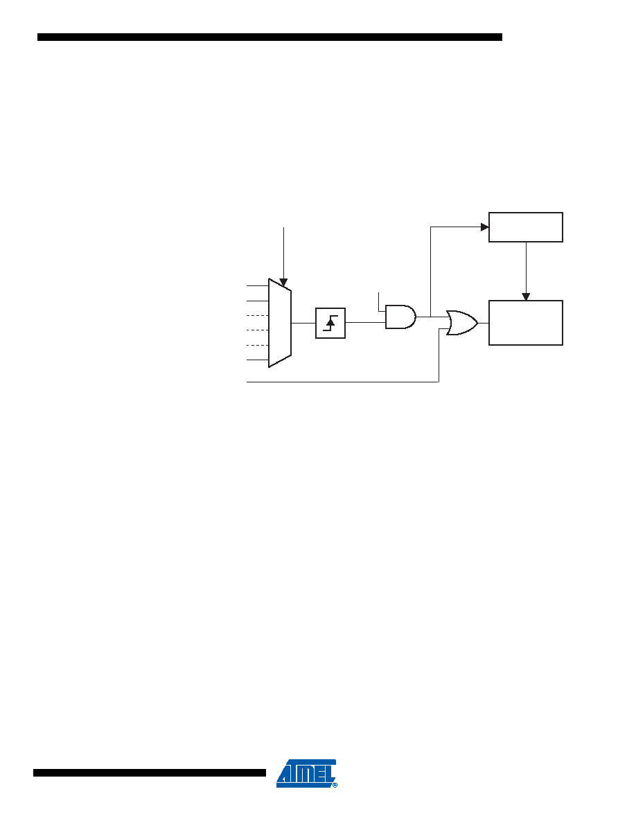
bits for a list of the trigger sources). When a positive edge occurs on the selected trigger signal,
the ADC prescaler is reset and a conversion is started. This provides a method of starting con-
versions at fixed intervals. If the trigger signal still is set when the conversion completes, a new
conversion will not be started. If another positive edge occurs on the trigger signal during con-
version, the edge will be ignored. Note that an Interrupt Flag will be set even if the specific
interrupt is disabled or the Global Interrupt Enable bit in SREG is cleared. A conversion can thus
be triggered without causing an interrupt. However, the Interrupt Flag must be cleared in order to
trigger a new conversion at the next interrupt event.
Figure 16-2. ADC Auto Trigger Logic
Using the ADC Interrupt Flag as a trigger source makes the ADC start a new conversion as soon
as the ongoing conversion has finished. The ADC then operates in Free Running mode, con-
stantly sampling and updating the ADC Data Register. The first conversion must be started by
writing a logical one to the ADSC bit in ADCSRA. In this mode the ADC will perform successive
conversions independently of whether the ADC Interrupt Flag, ADIF is cleared or not.
If Auto Triggering is enabled, single conversions can be started by writing ADSC in ADCSRA to
one. ADSC can also be used to determine if a conversion is in progress. The ADSC bit will be
read as one during a conversion, independently of how the conversion was started.
16.5
Prescaling and Conversion Timing
By default, the successive approximation circuitry requires an input clock frequency between 50
kHz and 200 kHz to get maximum resolution. If a lower resolution than 10 bits is needed, the
input clock frequency to the ADC can be higher than 200 kHz to get a higher sample rate. It is
not recommended to use a higher input clock frequency than 1 MHz.
The ADC module contains a prescaler, as illustrated in Figure 16-3 on page 120, which gener-
ates an acceptable ADC clock frequency from any CPU frequency above 100 kHz. The
prescaling is set by the ADPS bits in ADCSRA. The prescaler starts counting from the moment
the ADC is switched on by setting the ADEN bit in ADCSRA. The prescaler keeps running for as
long as the ADEN bit is set, and is continuously reset when ADEN is low.
ADSC
ADIF
SOURCE 1
SOURCE n
ADTS[2:0]
CONVERSION
LOGIC
PRESCALER
START
CLK
ADC
.
EDGE
DETECTOR
ADATE
相关PDF资料 |
PDF描述 |
|---|---|
| PIC16F870-E/SP | IC MCU CMOS 20MHZ 2K FLASH 28DIP |
| PIC16F870-E/SO | IC MCU CMOS 20MHZ 2K FLSH 28SOIC |
| PIC16LCE624-04/P | IC MCU OTP 1KX14 EE 18DIP |
| VI-BNP-IX-S | CONVERTER MOD DC/DC 13.8V 75W |
| PIC16LC711-04E/SS | IC MCU OTP 1KX14 A/D 20SSOP |
相关代理商/技术参数 |
参数描述 |
|---|---|
| PIC16F872-I/SO | 功能描述:8位微控制器 -MCU 3.5KB 128 RAM 22 I/O RoHS:否 制造商:Silicon Labs 核心:8051 处理器系列:C8051F39x 数据总线宽度:8 bit 最大时钟频率:50 MHz 程序存储器大小:16 KB 数据 RAM 大小:1 KB 片上 ADC:Yes 工作电源电压:1.8 V to 3.6 V 工作温度范围:- 40 C to + 105 C 封装 / 箱体:QFN-20 安装风格:SMD/SMT |
| PIC16F872-I/SO | 制造商:Microchip Technology Inc 功能描述:8BIT FLASH MCU SMD 16F872 SOIC28 |
| PIC16F872-I/SOG | 功能描述:8位微控制器 -MCU 3.5KB 128 RAM 22 I/O Lead Free Package RoHS:否 制造商:Silicon Labs 核心:8051 处理器系列:C8051F39x 数据总线宽度:8 bit 最大时钟频率:50 MHz 程序存储器大小:16 KB 数据 RAM 大小:1 KB 片上 ADC:Yes 工作电源电压:1.8 V to 3.6 V 工作温度范围:- 40 C to + 105 C 封装 / 箱体:QFN-20 安装风格:SMD/SMT |
| PIC16F872-I/SP | 功能描述:8位微控制器 -MCU 3.5KB 128 RAM 22 I/O RoHS:否 制造商:Silicon Labs 核心:8051 处理器系列:C8051F39x 数据总线宽度:8 bit 最大时钟频率:50 MHz 程序存储器大小:16 KB 数据 RAM 大小:1 KB 片上 ADC:Yes 工作电源电压:1.8 V to 3.6 V 工作温度范围:- 40 C to + 105 C 封装 / 箱体:QFN-20 安装风格:SMD/SMT |
| PIC16F872-I/SP | 制造商:Microchip Technology Inc 功能描述:IC 8BIT FLASH MCU 16F872 SDIL28 |
发布紧急采购,3分钟左右您将得到回复。