- 您现在的位置:买卖IC网 > PDF目录11455 > PIC16F872-E/SO (Microchip Technology)IC MCU CMOS 20MHZ 2K FLSH 28SOIC PDF资料下载
参数资料
| 型号: | PIC16F872-E/SO |
| 厂商: | Microchip Technology |
| 文件页数: | 7/167页 |
| 文件大小: | 0K |
| 描述: | IC MCU CMOS 20MHZ 2K FLSH 28SOIC |
| 产品培训模块: | Asynchronous Stimulus |
| 标准包装: | 27 |
| 系列: | PIC® 16F |
| 核心处理器: | PIC |
| 芯体尺寸: | 8-位 |
| 速度: | 20MHz |
| 连通性: | I²C,SPI |
| 外围设备: | 欠压检测/复位,POR,PWM,WDT |
| 输入/输出数: | 22 |
| 程序存储器容量: | 3.5KB(2K x 14) |
| 程序存储器类型: | 闪存 |
| EEPROM 大小: | 64 x 8 |
| RAM 容量: | 128 x 8 |
| 电压 - 电源 (Vcc/Vdd): | 4 V ~ 5.5 V |
| 数据转换器: | A/D 5x10b |
| 振荡器型: | 外部 |
| 工作温度: | -40°C ~ 125°C |
| 封装/外壳: | 28-SOIC(0.295",7.50mm 宽) |
| 包装: | 管件 |
第1页第2页第3页第4页第5页第6页当前第7页第8页第9页第10页第11页第12页第13页第14页第15页第16页第17页第18页第19页第20页第21页第22页第23页第24页第25页第26页第27页第28页第29页第30页第31页第32页第33页第34页第35页第36页第37页第38页第39页第40页第41页第42页第43页第44页第45页第46页第47页第48页第49页第50页第51页第52页第53页第54页第55页第56页第57页第58页第59页第60页第61页第62页第63页第64页第65页第66页第67页第68页第69页第70页第71页第72页第73页第74页第75页第76页第77页第78页第79页第80页第81页第82页第83页第84页第85页第86页第87页第88页第89页第90页第91页第92页第93页第94页第95页第96页第97页第98页第99页第100页第101页第102页第103页第104页第105页第106页第107页第108页第109页第110页第111页第112页第113页第114页第115页第116页第117页第118页第119页第120页第121页第122页第123页第124页第125页第126页第127页第128页第129页第130页第131页第132页第133页第134页第135页第136页第137页第138页第139页第140页第141页第142页第143页第144页第145页第146页第147页第148页第149页第150页第151页第152页第153页第154页第155页第156页第157页第158页第159页第160页第161页第162页第163页第164页第165页第166页第167页
104
8048C–AVR–02/12
ATtiny43U
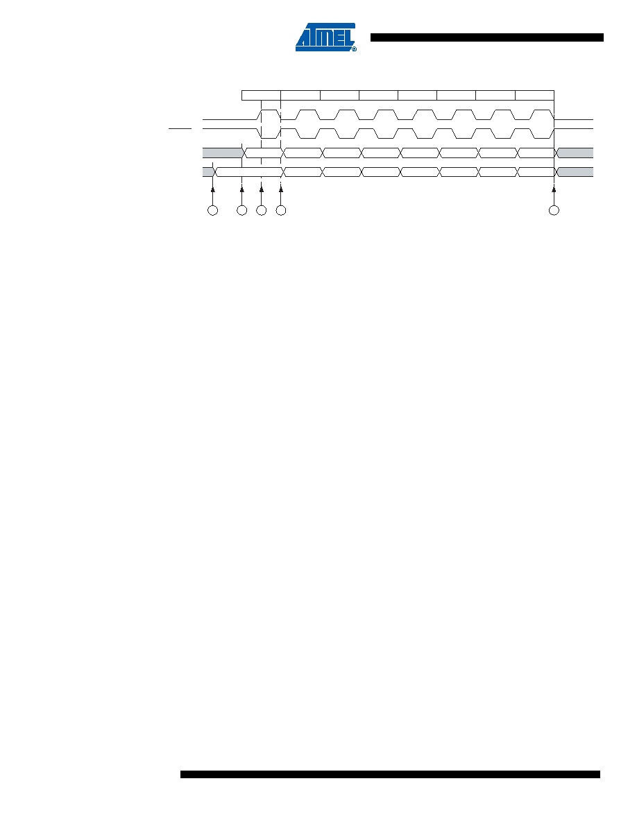
Figure 14-3. Three-wire Mode, Timing Diagram
The three-wire mode timing is shown in Figure 14-3 At the top of the figure is a USCK cycle ref-
erence. One bit is shifted into the USI Data Register (USIDR) for each of these cycles. The
USCK timing is shown for both external clock modes. In external clock mode 0 (USICS0 = 0), DI
is sampled at positive edges, and DO is changed (USI Data Register is shifted by one) at nega-
tive edges. In external clock mode 1 (USICS0 = 1) the opposite edges with respect to mode 0
are used. In other words, data is sampled at negative and output is changed at positive edges.
The USI clock modes corresponds to the SPI data mode 0 and 1.
Referring to the timing diagram (Figure 14-3), a bus transfer involves the following steps:
1.
The slave and master devices set up their data outputs and, depending on the protocol
used, enable their output drivers (mark A and B). The output is set up by writing the
data to be transmitted to the USI Data Register. The output is enabled by setting the
corresponding bit in the Data Direction Register of Port A. Note that there is not a pre-
ferred order of points A and B in the figure, but both must be at least one half USCK
cycle before point C, where the data is sampled. This is in order to ensure that the data
setup requirement is satisfied. The 4-bit counter is reset to zero.
2.
The master software generates a clock pulse by toggling the USCK line twice (C and
D). The bit values on the data input (DI) pins are sampled by the USI on the first edge
(C), and the data output is changed on the opposite edge (D). The 4-bit counter will
count both edges.
3.
Step 2. is repeated eight times for a complete register (byte) transfer.
4.
After eight clock pulses (i.e., 16 clock edges) the counter will overflow and indicate that
the transfer has been completed. If USI Buffer Registers are not used the data bytes
that have been transferred must now be processed before a new transfer can be initi-
ated. The overflow interrupt will wake up the processor if it is set to Idle mode.
Depending on the protocol used the slave device can now set its output to high
impedance.
14.3.2
SPI Master Operation Example
The following code demonstrates how to use the USI module as a SPI Master:
SPITransfer:
out
USIDR,r16
ldi
r16,(1<<USIOIF)
out
USISR,r16
ldi
r17,(1<<USIWM0)|(1<<USICS1)|(1<<USICLK)|(1<<USITC)
<continues>
MSB
654321
LSB
1
2
3
4
5
6
7
8
654321
LSB
USCK
DO
DI
D
C
B
A
E
CYCLE ( Reference )
相关PDF资料 |
PDF描述 |
|---|---|
| PIC16F870-E/SP | IC MCU CMOS 20MHZ 2K FLASH 28DIP |
| PIC16F870-E/SO | IC MCU CMOS 20MHZ 2K FLSH 28SOIC |
| PIC16LCE624-04/P | IC MCU OTP 1KX14 EE 18DIP |
| VI-BNP-IX-S | CONVERTER MOD DC/DC 13.8V 75W |
| PIC16LC711-04E/SS | IC MCU OTP 1KX14 A/D 20SSOP |
相关代理商/技术参数 |
参数描述 |
|---|---|
| PIC16F872-I/SO | 功能描述:8位微控制器 -MCU 3.5KB 128 RAM 22 I/O RoHS:否 制造商:Silicon Labs 核心:8051 处理器系列:C8051F39x 数据总线宽度:8 bit 最大时钟频率:50 MHz 程序存储器大小:16 KB 数据 RAM 大小:1 KB 片上 ADC:Yes 工作电源电压:1.8 V to 3.6 V 工作温度范围:- 40 C to + 105 C 封装 / 箱体:QFN-20 安装风格:SMD/SMT |
| PIC16F872-I/SO | 制造商:Microchip Technology Inc 功能描述:8BIT FLASH MCU SMD 16F872 SOIC28 |
| PIC16F872-I/SOG | 功能描述:8位微控制器 -MCU 3.5KB 128 RAM 22 I/O Lead Free Package RoHS:否 制造商:Silicon Labs 核心:8051 处理器系列:C8051F39x 数据总线宽度:8 bit 最大时钟频率:50 MHz 程序存储器大小:16 KB 数据 RAM 大小:1 KB 片上 ADC:Yes 工作电源电压:1.8 V to 3.6 V 工作温度范围:- 40 C to + 105 C 封装 / 箱体:QFN-20 安装风格:SMD/SMT |
| PIC16F872-I/SP | 功能描述:8位微控制器 -MCU 3.5KB 128 RAM 22 I/O RoHS:否 制造商:Silicon Labs 核心:8051 处理器系列:C8051F39x 数据总线宽度:8 bit 最大时钟频率:50 MHz 程序存储器大小:16 KB 数据 RAM 大小:1 KB 片上 ADC:Yes 工作电源电压:1.8 V to 3.6 V 工作温度范围:- 40 C to + 105 C 封装 / 箱体:QFN-20 安装风格:SMD/SMT |
| PIC16F872-I/SP | 制造商:Microchip Technology Inc 功能描述:IC 8BIT FLASH MCU 16F872 SDIL28 |
发布紧急采购,3分钟左右您将得到回复。