- 您现在的位置:买卖IC网 > PDF目录11455 > PIC16F872-E/SO (Microchip Technology)IC MCU CMOS 20MHZ 2K FLSH 28SOIC PDF资料下载
参数资料
| 型号: | PIC16F872-E/SO |
| 厂商: | Microchip Technology |
| 文件页数: | 36/167页 |
| 文件大小: | 0K |
| 描述: | IC MCU CMOS 20MHZ 2K FLSH 28SOIC |
| 产品培训模块: | Asynchronous Stimulus |
| 标准包装: | 27 |
| 系列: | PIC® 16F |
| 核心处理器: | PIC |
| 芯体尺寸: | 8-位 |
| 速度: | 20MHz |
| 连通性: | I²C,SPI |
| 外围设备: | 欠压检测/复位,POR,PWM,WDT |
| 输入/输出数: | 22 |
| 程序存储器容量: | 3.5KB(2K x 14) |
| 程序存储器类型: | 闪存 |
| EEPROM 大小: | 64 x 8 |
| RAM 容量: | 128 x 8 |
| 电压 - 电源 (Vcc/Vdd): | 4 V ~ 5.5 V |
| 数据转换器: | A/D 5x10b |
| 振荡器型: | 外部 |
| 工作温度: | -40°C ~ 125°C |
| 封装/外壳: | 28-SOIC(0.295",7.50mm 宽) |
| 包装: | 管件 |
第1页第2页第3页第4页第5页第6页第7页第8页第9页第10页第11页第12页第13页第14页第15页第16页第17页第18页第19页第20页第21页第22页第23页第24页第25页第26页第27页第28页第29页第30页第31页第32页第33页第34页第35页当前第36页第37页第38页第39页第40页第41页第42页第43页第44页第45页第46页第47页第48页第49页第50页第51页第52页第53页第54页第55页第56页第57页第58页第59页第60页第61页第62页第63页第64页第65页第66页第67页第68页第69页第70页第71页第72页第73页第74页第75页第76页第77页第78页第79页第80页第81页第82页第83页第84页第85页第86页第87页第88页第89页第90页第91页第92页第93页第94页第95页第96页第97页第98页第99页第100页第101页第102页第103页第104页第105页第106页第107页第108页第109页第110页第111页第112页第113页第114页第115页第116页第117页第118页第119页第120页第121页第122页第123页第124页第125页第126页第127页第128页第129页第130页第131页第132页第133页第134页第135页第136页第137页第138页第139页第140页第141页第142页第143页第144页第145页第146页第147页第148页第149页第150页第151页第152页第153页第154页第155页第156页第157页第158页第159页第160页第161页第162页第163页第164页第165页第166页第167页
131
8048C–AVR–02/12
ATtiny43U
16.13.3.2
ADLAR = 1
When an ADC conversion is complete, the result is found in these two registers.
When ADCL is read, the ADC Data Register is not updated until ADCH is read. Consequently, if
the result is left adjusted and no more than 8-bit precision is required, it is sufficient to read
ADCH. Otherwise, ADCL must be read first, then ADCH.
The ADLAR bit in ADCSRB, and the MUXn bits in ADMUX affect the way the result is read from
the registers. If ADLAR is set, the result is left adjusted. If ADLAR is cleared (default), the result
is right adjusted.
ADC[9:0]: ADC Conversion Result
These bits represent the result from the conversion, as detailed in “ADC Conversion Result” on
16.13.4
ADCSRB – ADC Control and Status Register B
Bit 5 – Res: Reserved Bit
This bit is reserved and will always read what was written.
Bit 4 – ADLAR: ADC Left Adjust Result
The ADLAR bit affects the presentation of the ADC conversion result in the ADC Data Register.
Write one to ADLAR to left adjust the result. Otherwise, the result is right adjusted. Changing the
ADLAR bit will affect the ADC Data Register immediately, regardless of any ongoing conver-
sions. For a comple the description of this bit, see “ADCL and ADCH – ADC Data Register” on
Bit 3 – Res: Reserved Bit
This bit is reserved and will always read what was written.
Bits 2:0 – ADTS[2:0]: ADC Auto Trigger Source
If ADATE in ADCSRA is written to one, the value of these bits selects which source will trigger
an ADC conversion. If ADATE is cleared, the ADTS[2:0] settings will have no effect. A conver-
sion will be triggered by the rising edge of the selected Interrupt Flag. Note that switching from a
trigger source that is cleared to a trigger source that is set, will generate a positive edge on the
Bit
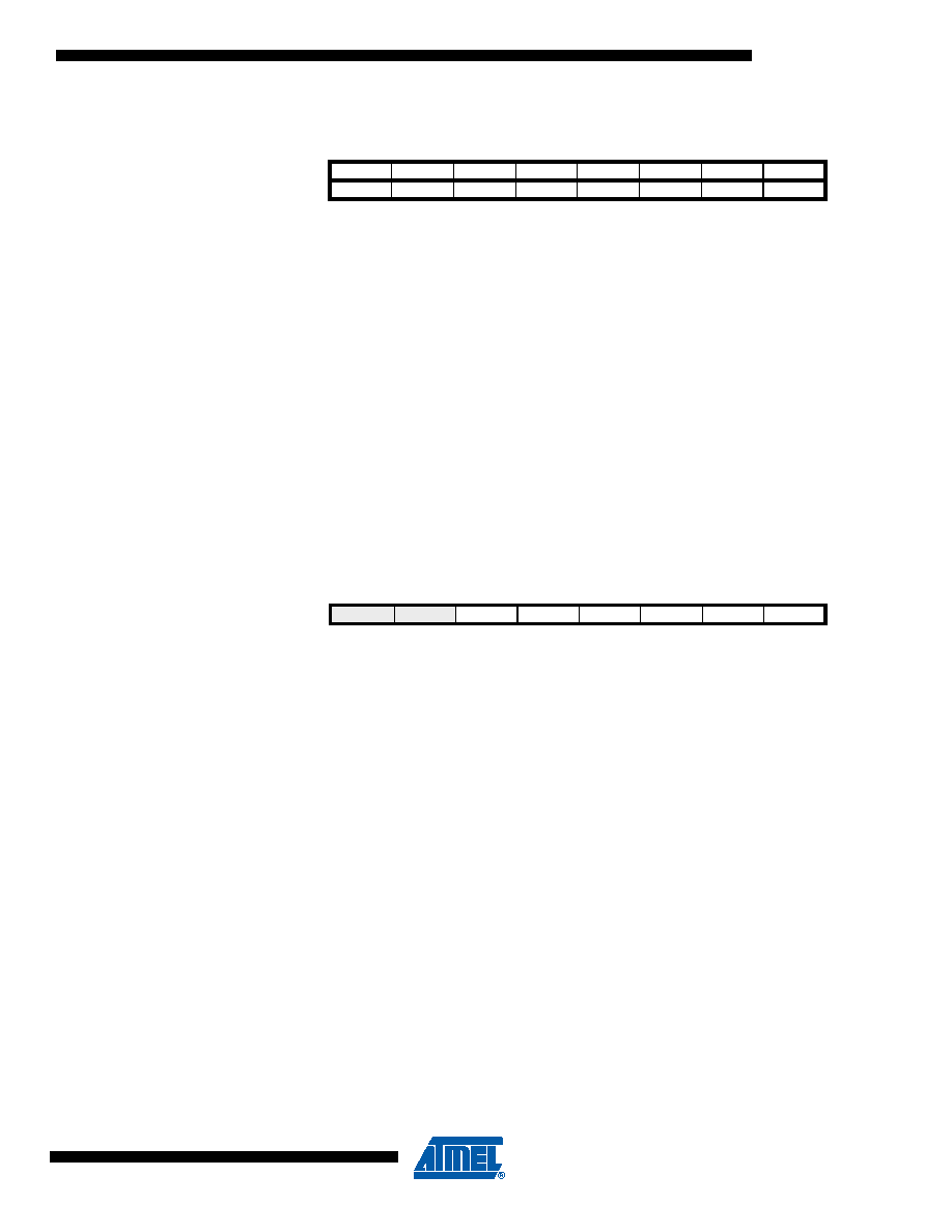
151413121110
9
8
ADC9
ADC8
ADC7
ADC6
ADC5
ADC4
ADC3
ADC2
ADCH
ADC1
ADC0
–
ADCL
765
43
21
0
Read/Write
R
RR
R
Initial Value
0
000
00
0
Bit
7
6543
210
BS
ACME
–
ADLAR
–
ADTS2
ADTS1
ADTS0
ADCSRB
Read/Write
R
R/W
R
R/W
R
R/W
Initial Value
0
0000
000
相关PDF资料 |
PDF描述 |
|---|---|
| PIC16F870-E/SP | IC MCU CMOS 20MHZ 2K FLASH 28DIP |
| PIC16F870-E/SO | IC MCU CMOS 20MHZ 2K FLSH 28SOIC |
| PIC16LCE624-04/P | IC MCU OTP 1KX14 EE 18DIP |
| VI-BNP-IX-S | CONVERTER MOD DC/DC 13.8V 75W |
| PIC16LC711-04E/SS | IC MCU OTP 1KX14 A/D 20SSOP |
相关代理商/技术参数 |
参数描述 |
|---|---|
| PIC16F872-I/SO | 功能描述:8位微控制器 -MCU 3.5KB 128 RAM 22 I/O RoHS:否 制造商:Silicon Labs 核心:8051 处理器系列:C8051F39x 数据总线宽度:8 bit 最大时钟频率:50 MHz 程序存储器大小:16 KB 数据 RAM 大小:1 KB 片上 ADC:Yes 工作电源电压:1.8 V to 3.6 V 工作温度范围:- 40 C to + 105 C 封装 / 箱体:QFN-20 安装风格:SMD/SMT |
| PIC16F872-I/SO | 制造商:Microchip Technology Inc 功能描述:8BIT FLASH MCU SMD 16F872 SOIC28 |
| PIC16F872-I/SOG | 功能描述:8位微控制器 -MCU 3.5KB 128 RAM 22 I/O Lead Free Package RoHS:否 制造商:Silicon Labs 核心:8051 处理器系列:C8051F39x 数据总线宽度:8 bit 最大时钟频率:50 MHz 程序存储器大小:16 KB 数据 RAM 大小:1 KB 片上 ADC:Yes 工作电源电压:1.8 V to 3.6 V 工作温度范围:- 40 C to + 105 C 封装 / 箱体:QFN-20 安装风格:SMD/SMT |
| PIC16F872-I/SP | 功能描述:8位微控制器 -MCU 3.5KB 128 RAM 22 I/O RoHS:否 制造商:Silicon Labs 核心:8051 处理器系列:C8051F39x 数据总线宽度:8 bit 最大时钟频率:50 MHz 程序存储器大小:16 KB 数据 RAM 大小:1 KB 片上 ADC:Yes 工作电源电压:1.8 V to 3.6 V 工作温度范围:- 40 C to + 105 C 封装 / 箱体:QFN-20 安装风格:SMD/SMT |
| PIC16F872-I/SP | 制造商:Microchip Technology Inc 功能描述:IC 8BIT FLASH MCU 16F872 SDIL28 |
发布紧急采购,3分钟左右您将得到回复。