- 您现在的位置:买卖IC网 > PDF目录11602 > PIC16LF1824-E/ML (Microchip Technology)IC MCU 8BIT 7KB FLASH 16QFN PDF资料下载
参数资料
| 型号: | PIC16LF1824-E/ML |
| 厂商: | Microchip Technology |
| 文件页数: | 12/101页 |
| 文件大小: | 0K |
| 描述: | IC MCU 8BIT 7KB FLASH 16QFN |
| 标准包装: | 91 |
| 系列: | PIC® XLP™ mTouch™ 16F |
| 核心处理器: | PIC |
| 芯体尺寸: | 8-位 |
| 速度: | 32MHz |
| 连通性: | I²C,SPI,UART/USART |
| 外围设备: | 欠压检测/复位,POR,PWM,WDT |
| 输入/输出数: | 11 |
| 程序存储器容量: | 7KB(4K x 14) |
| 程序存储器类型: | 闪存 |
| EEPROM 大小: | 256 x 8 |
| RAM 容量: | 256 x 8 |
| 电压 - 电源 (Vcc/Vdd): | 1.8 V ~ 3.6 V |
| 数据转换器: | A/D 8x10b |
| 振荡器型: | 内部 |
| 工作温度: | -40°C ~ 125°C |
| 封装/外壳: | 16-VQFN 裸露焊盘 |
| 包装: | 管件 |
第1页第2页第3页第4页第5页第6页第7页第8页第9页第10页第11页当前第12页第13页第14页第15页第16页第17页第18页第19页第20页第21页第22页第23页第24页第25页第26页第27页第28页第29页第30页第31页第32页第33页第34页第35页第36页第37页第38页第39页第40页第41页第42页第43页第44页第45页第46页第47页第48页第49页第50页第51页第52页第53页第54页第55页第56页第57页第58页第59页第60页第61页第62页第63页第64页第65页第66页第67页第68页第69页第70页第71页第72页第73页第74页第75页第76页第77页第78页第79页第80页第81页第82页第83页第84页第85页第86页第87页第88页第89页第90页第91页第92页第93页第94页第95页第96页第97页第98页第99页第100页第101页
159
2552K–AVR–04/11
ATmega329/3290/649/6490
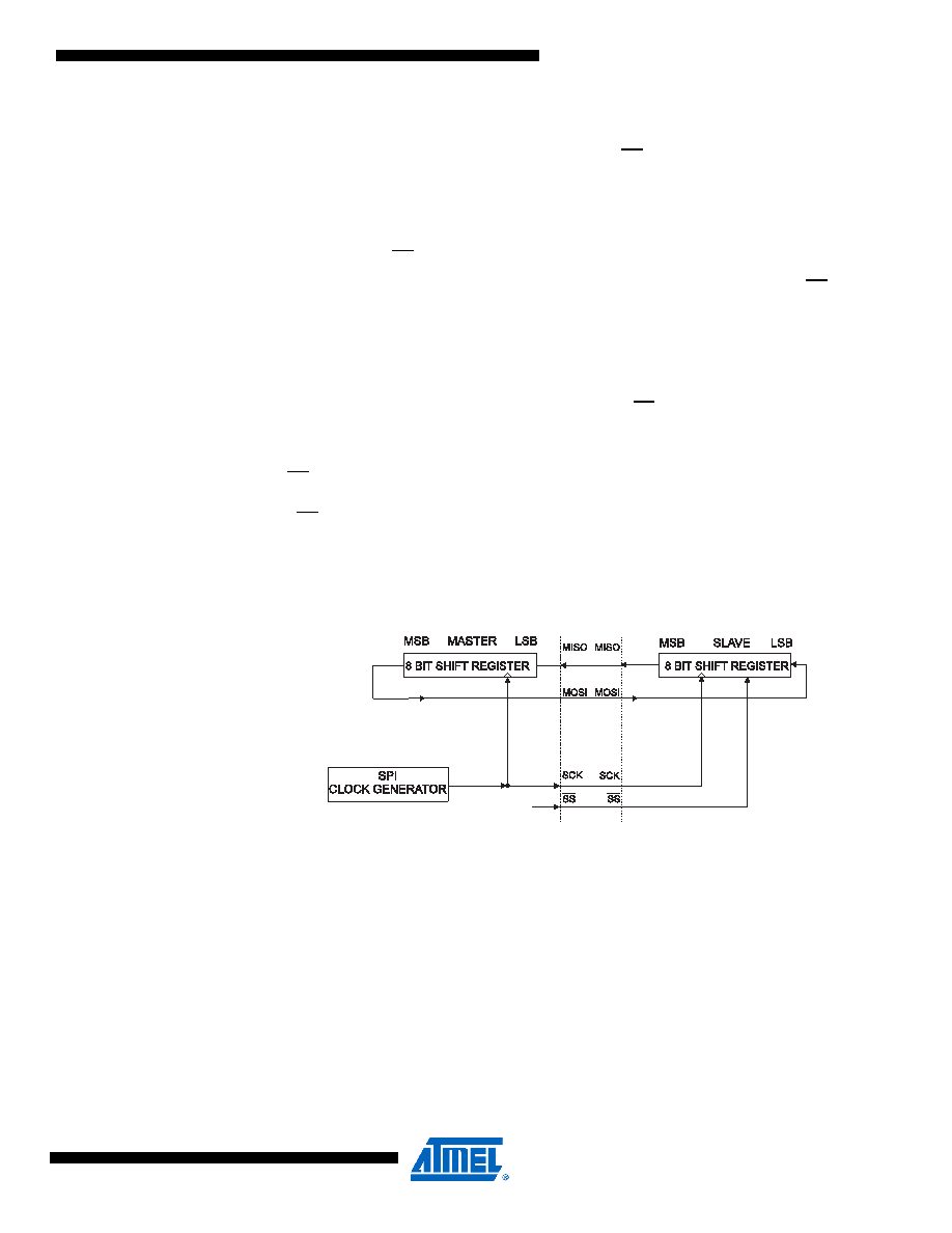
The interconnection between Master and Slave CPUs with SPI is shown in Figure 18-2. The sys-
tem consists of two shift Registers, and a Master clock generator. The SPI Master initiates the
communication cycle when pulling low the Slave Select SS pin of the desired Slave. Master and
Slave prepare the data to be sent in their respective shift Registers, and the Master generates
the required clock pulses on the SCK line to interchange data. Data is always shifted from Mas-
ter to Slave on the Master Out – Slave In, MOSI, line, and from Slave to Master on the Master In
– Slave Out, MISO, line. After each data packet, the Master will synchronize the Slave by pulling
high the Slave Select, SS, line.
When configured as a Master, the SPI interface has no automatic control of the SS line. This
must be handled by user software before communication can start. When this is done, writing a
byte to the SPI Data Register starts the SPI clock generator, and the hardware shifts the eight
bits into the Slave. After shifting one byte, the SPI clock generator stops, setting the end of
Transmission Flag (SPIF). If the SPI Interrupt Enable bit (SPIE) in the SPCR Register is set, an
interrupt is requested. The Master may continue to shift the next byte by writing it into SPDR, or
signal the end of packet by pulling high the Slave Select, SS line. The last incoming byte will be
kept in the Buffer Register for later use.
When configured as a Slave, the SPI interface will remain sleeping with MISO tri-stated as long
as the SS pin is driven high. In this state, software may update the contents of the SPI Data
Register, SPDR, but the data will not be shifted out by incoming clock pulses on the SCK pin
until the SS pin is driven low. As one byte has been completely shifted, the end of Transmission
Flag, SPIF is set. If the SPI Interrupt Enable bit, SPIE, in the SPCR Register is set, an interrupt
is requested. The Slave may continue to place new data to be sent into SPDR before reading
the incoming data. The last incoming byte will be kept in the Buffer Register for later use.
Figure 18-2. SPI Master-slave Interconnection
The system is single buffered in the transmit direction and double buffered in the receive direc-
tion. This means that bytes to be transmitted cannot be written to the SPI Data Register before
the entire shift cycle is completed. When receiving data, however, a received character must be
read from the SPI Data Register before the next character has been completely shifted in. Oth-
erwise, the first byte is lost.
In SPI Slave mode, the control logic will sample the incoming signal of the SCK pin. To ensure
correct sampling of the clock signal, the minimum low and high period should be:
Low period: longer than 2 CPU clock cycles.
High period: longer than 2 CPU clock cycles.
SHIFT
ENABLE
相关PDF资料 |
PDF描述 |
|---|---|
| D38999/20FJ7SN | CONN RCPT 99POS WALL MNT W/SCKT |
| PIC16LF723AT-I/MV | MCU 8BIT 4K FLASH XLP 28-UQFN |
| PIC16F723AT-I/MV | MCU 8BIT 4K FLASH XLP 28-UQFN |
| D38999/26WJ7SA | CONN PLUG 99POS STRAIGHT W/SCKT |
| PIC16LF1826T-I/SO | MCU 8BIT 2K FLASH 18SOIC |
相关代理商/技术参数 |
参数描述 |
|---|---|
| PIC16LF1824-I/ML | 功能描述:8位微控制器 -MCU 7KB Flash 256B RAM 32 MHz Int Osc Core RoHS:否 制造商:Silicon Labs 核心:8051 处理器系列:C8051F39x 数据总线宽度:8 bit 最大时钟频率:50 MHz 程序存储器大小:16 KB 数据 RAM 大小:1 KB 片上 ADC:Yes 工作电源电压:1.8 V to 3.6 V 工作温度范围:- 40 C to + 105 C 封装 / 箱体:QFN-20 安装风格:SMD/SMT |
| PIC16LF1824-I/P | 功能描述:8位微控制器 -MCU 7KB Flash 256B RAM 32 MHz Int Osc Core RoHS:否 制造商:Silicon Labs 核心:8051 处理器系列:C8051F39x 数据总线宽度:8 bit 最大时钟频率:50 MHz 程序存储器大小:16 KB 数据 RAM 大小:1 KB 片上 ADC:Yes 工作电源电压:1.8 V to 3.6 V 工作温度范围:- 40 C to + 105 C 封装 / 箱体:QFN-20 安装风格:SMD/SMT |
| PIC16LF1824-I/SL | 功能描述:8位微控制器 -MCU 7KB Flash 256B RAM 32 MHz Int Osc Core RoHS:否 制造商:Silicon Labs 核心:8051 处理器系列:C8051F39x 数据总线宽度:8 bit 最大时钟频率:50 MHz 程序存储器大小:16 KB 数据 RAM 大小:1 KB 片上 ADC:Yes 工作电源电压:1.8 V to 3.6 V 工作温度范围:- 40 C to + 105 C 封装 / 箱体:QFN-20 安装风格:SMD/SMT |
| PIC16LF1824-I/ST | 功能描述:8位微控制器 -MCU 7KB Flash 256B RAM 32 MHz Int Osc Core RoHS:否 制造商:Silicon Labs 核心:8051 处理器系列:C8051F39x 数据总线宽度:8 bit 最大时钟频率:50 MHz 程序存储器大小:16 KB 数据 RAM 大小:1 KB 片上 ADC:Yes 工作电源电压:1.8 V to 3.6 V 工作温度范围:- 40 C to + 105 C 封装 / 箱体:QFN-20 安装风格:SMD/SMT |
| PIC16LF1824T39A-I/ST | 制造商:Microchip Technology 功能描述:MCU 8-bit PIC16 PIC RISC 7KB Flash 2.5V/3.3V 20-Pin TSSOP 制造商:Microchip Technology Inc 功能描述:PIC16LF1824 MICROCONTROLLER WITH 300-900 MHZ TRANSMITTER - Rail/Tube 制造商:Microchip Technology Inc 功能描述:IC MCU 8BIT FLASH 20TSSOP 制造商:Microchip Technology Inc 功能描述:PIC16LF1824 Microcontroller |
发布紧急采购,3分钟左右您将得到回复。