- 您现在的位置:买卖IC网 > PDF目录11602 > PIC16LF1824-E/ML (Microchip Technology)IC MCU 8BIT 7KB FLASH 16QFN PDF资料下载
参数资料
| 型号: | PIC16LF1824-E/ML |
| 厂商: | Microchip Technology |
| 文件页数: | 27/101页 |
| 文件大小: | 0K |
| 描述: | IC MCU 8BIT 7KB FLASH 16QFN |
| 标准包装: | 91 |
| 系列: | PIC® XLP™ mTouch™ 16F |
| 核心处理器: | PIC |
| 芯体尺寸: | 8-位 |
| 速度: | 32MHz |
| 连通性: | I²C,SPI,UART/USART |
| 外围设备: | 欠压检测/复位,POR,PWM,WDT |
| 输入/输出数: | 11 |
| 程序存储器容量: | 7KB(4K x 14) |
| 程序存储器类型: | 闪存 |
| EEPROM 大小: | 256 x 8 |
| RAM 容量: | 256 x 8 |
| 电压 - 电源 (Vcc/Vdd): | 1.8 V ~ 3.6 V |
| 数据转换器: | A/D 8x10b |
| 振荡器型: | 内部 |
| 工作温度: | -40°C ~ 125°C |
| 封装/外壳: | 16-VQFN 裸露焊盘 |
| 包装: | 管件 |
第1页第2页第3页第4页第5页第6页第7页第8页第9页第10页第11页第12页第13页第14页第15页第16页第17页第18页第19页第20页第21页第22页第23页第24页第25页第26页当前第27页第28页第29页第30页第31页第32页第33页第34页第35页第36页第37页第38页第39页第40页第41页第42页第43页第44页第45页第46页第47页第48页第49页第50页第51页第52页第53页第54页第55页第56页第57页第58页第59页第60页第61页第62页第63页第64页第65页第66页第67页第68页第69页第70页第71页第72页第73页第74页第75页第76页第77页第78页第79页第80页第81页第82页第83页第84页第85页第86页第87页第88页第89页第90页第91页第92页第93页第94页第95页第96页第97页第98页第99页第100页第101页
172
2552K–AVR–04/11
ATmega329/3290/649/6490
19.3.4
Synchronous Clock Operation
When synchronous mode is used (UMSELn = 1), the XCK pin will be used as either clock input
(Slave) or clock output (Master). The dependency between the clock edges and data sampling
or data change is the same. The basic principle is that data input (on RxD) is sampled at the
opposite XCK clock edge of the edge the data output (TxD) is changed.
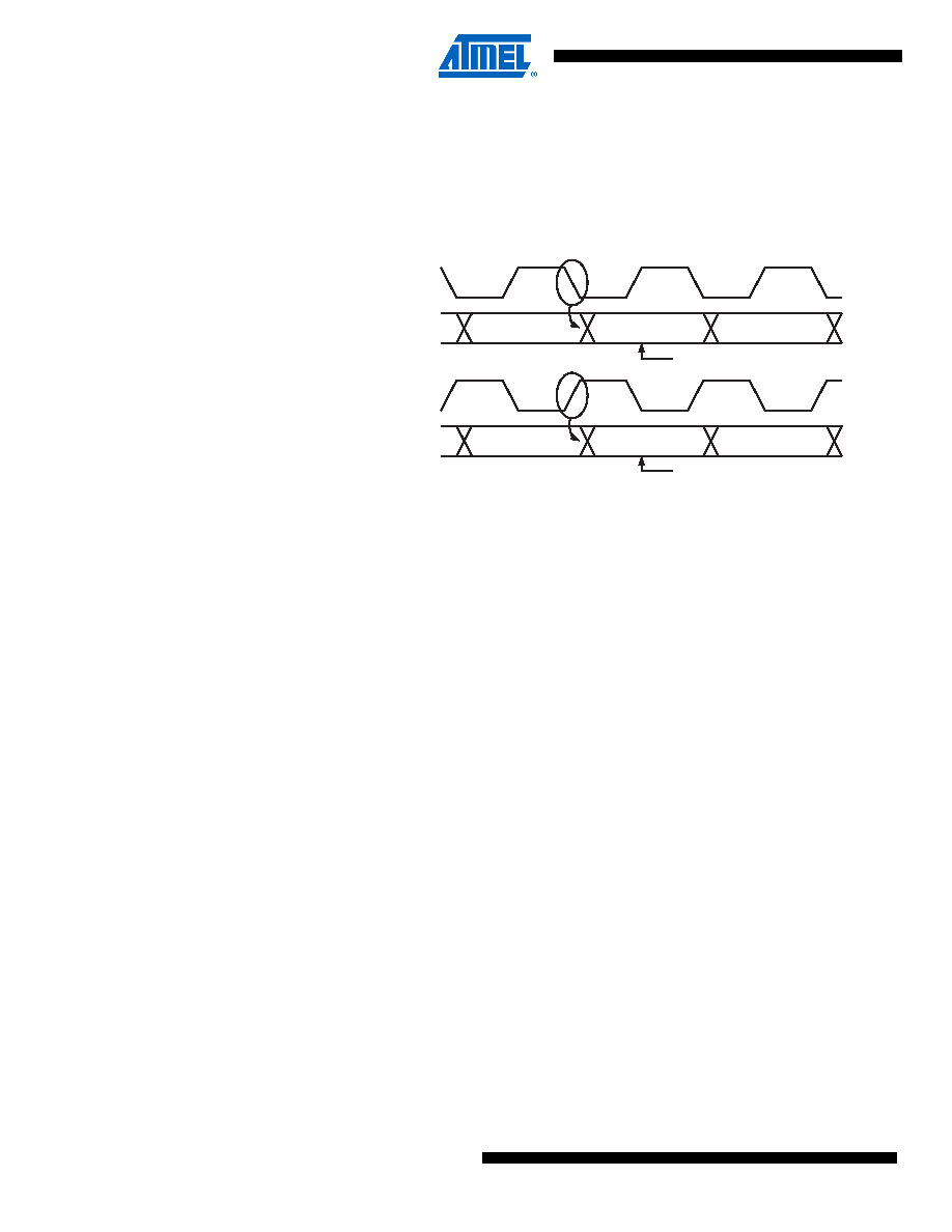
Figure 19-3. Synchronous Mode XCK Timing.
The UCPOLn bit UCRSC selects which XCK clock edge is used for data sampling and which is
used for data change. As Figure 19-3 shows, when UCPOLn is zero the data will be changed at
rising XCK edge and sampled at falling XCK edge. If UCPOLn is set, the data will be changed at
falling XCK edge and sampled at rising XCK edge.
19.4
Frame Formats
A serial frame is defined to be one character of data bits with synchronization bits (start and stop
bits), and optionally a parity bit for error checking. The USART accepts all 30 combinations of
the following as valid frame formats:
1 start bit
5, 6, 7, 8, or 9 data bits
no, even or odd parity bit
1 or 2 stop bits
A frame starts with the start bit followed by the least significant data bit. Then the next data bits,
up to a total of nine, are succeeding, ending with the most significant bit. If enabled, the parity bit
is inserted after the data bits, before the stop bits. When a complete frame is transmitted, it can
be directly followed by a new frame, or the communication line can be set to an idle (high) state.
Figure 19-4 illustrates the possible combinations of the frame formats. Bits inside brackets are
optional.
RxD / TxD
XCK
RxD / TxD
XCK
UCPOL = 0
UCPOL = 1
Sample
相关PDF资料 |
PDF描述 |
|---|---|
| D38999/20FJ7SN | CONN RCPT 99POS WALL MNT W/SCKT |
| PIC16LF723AT-I/MV | MCU 8BIT 4K FLASH XLP 28-UQFN |
| PIC16F723AT-I/MV | MCU 8BIT 4K FLASH XLP 28-UQFN |
| D38999/26WJ7SA | CONN PLUG 99POS STRAIGHT W/SCKT |
| PIC16LF1826T-I/SO | MCU 8BIT 2K FLASH 18SOIC |
相关代理商/技术参数 |
参数描述 |
|---|---|
| PIC16LF1824-I/ML | 功能描述:8位微控制器 -MCU 7KB Flash 256B RAM 32 MHz Int Osc Core RoHS:否 制造商:Silicon Labs 核心:8051 处理器系列:C8051F39x 数据总线宽度:8 bit 最大时钟频率:50 MHz 程序存储器大小:16 KB 数据 RAM 大小:1 KB 片上 ADC:Yes 工作电源电压:1.8 V to 3.6 V 工作温度范围:- 40 C to + 105 C 封装 / 箱体:QFN-20 安装风格:SMD/SMT |
| PIC16LF1824-I/P | 功能描述:8位微控制器 -MCU 7KB Flash 256B RAM 32 MHz Int Osc Core RoHS:否 制造商:Silicon Labs 核心:8051 处理器系列:C8051F39x 数据总线宽度:8 bit 最大时钟频率:50 MHz 程序存储器大小:16 KB 数据 RAM 大小:1 KB 片上 ADC:Yes 工作电源电压:1.8 V to 3.6 V 工作温度范围:- 40 C to + 105 C 封装 / 箱体:QFN-20 安装风格:SMD/SMT |
| PIC16LF1824-I/SL | 功能描述:8位微控制器 -MCU 7KB Flash 256B RAM 32 MHz Int Osc Core RoHS:否 制造商:Silicon Labs 核心:8051 处理器系列:C8051F39x 数据总线宽度:8 bit 最大时钟频率:50 MHz 程序存储器大小:16 KB 数据 RAM 大小:1 KB 片上 ADC:Yes 工作电源电压:1.8 V to 3.6 V 工作温度范围:- 40 C to + 105 C 封装 / 箱体:QFN-20 安装风格:SMD/SMT |
| PIC16LF1824-I/ST | 功能描述:8位微控制器 -MCU 7KB Flash 256B RAM 32 MHz Int Osc Core RoHS:否 制造商:Silicon Labs 核心:8051 处理器系列:C8051F39x 数据总线宽度:8 bit 最大时钟频率:50 MHz 程序存储器大小:16 KB 数据 RAM 大小:1 KB 片上 ADC:Yes 工作电源电压:1.8 V to 3.6 V 工作温度范围:- 40 C to + 105 C 封装 / 箱体:QFN-20 安装风格:SMD/SMT |
| PIC16LF1824T39A-I/ST | 制造商:Microchip Technology 功能描述:MCU 8-bit PIC16 PIC RISC 7KB Flash 2.5V/3.3V 20-Pin TSSOP 制造商:Microchip Technology Inc 功能描述:PIC16LF1824 MICROCONTROLLER WITH 300-900 MHZ TRANSMITTER - Rail/Tube 制造商:Microchip Technology Inc 功能描述:IC MCU 8BIT FLASH 20TSSOP 制造商:Microchip Technology Inc 功能描述:PIC16LF1824 Microcontroller |
发布紧急采购,3分钟左右您将得到回复。