- 您现在的位置:买卖IC网 > PDF目录11602 > PIC16LF1824-E/ML (Microchip Technology)IC MCU 8BIT 7KB FLASH 16QFN PDF资料下载
参数资料
| 型号: | PIC16LF1824-E/ML |
| 厂商: | Microchip Technology |
| 文件页数: | 64/101页 |
| 文件大小: | 0K |
| 描述: | IC MCU 8BIT 7KB FLASH 16QFN |
| 标准包装: | 91 |
| 系列: | PIC® XLP™ mTouch™ 16F |
| 核心处理器: | PIC |
| 芯体尺寸: | 8-位 |
| 速度: | 32MHz |
| 连通性: | I²C,SPI,UART/USART |
| 外围设备: | 欠压检测/复位,POR,PWM,WDT |
| 输入/输出数: | 11 |
| 程序存储器容量: | 7KB(4K x 14) |
| 程序存储器类型: | 闪存 |
| EEPROM 大小: | 256 x 8 |
| RAM 容量: | 256 x 8 |
| 电压 - 电源 (Vcc/Vdd): | 1.8 V ~ 3.6 V |
| 数据转换器: | A/D 8x10b |
| 振荡器型: | 内部 |
| 工作温度: | -40°C ~ 125°C |
| 封装/外壳: | 16-VQFN 裸露焊盘 |
| 包装: | 管件 |
第1页第2页第3页第4页第5页第6页第7页第8页第9页第10页第11页第12页第13页第14页第15页第16页第17页第18页第19页第20页第21页第22页第23页第24页第25页第26页第27页第28页第29页第30页第31页第32页第33页第34页第35页第36页第37页第38页第39页第40页第41页第42页第43页第44页第45页第46页第47页第48页第49页第50页第51页第52页第53页第54页第55页第56页第57页第58页第59页第60页第61页第62页第63页当前第64页第65页第66页第67页第68页第69页第70页第71页第72页第73页第74页第75页第76页第77页第78页第79页第80页第81页第82页第83页第84页第85页第86页第87页第88页第89页第90页第91页第92页第93页第94页第95页第96页第97页第98页第99页第100页第101页
205
2552K–AVR–04/11
ATmega329/3290/649/6490
Note:
1. The DI and USCK pins are renamed to Serial Data (SDA) and Serial Clock (SCL) respectively
to avoid confusion between the modes of operation.
Bit 3..2 – USICS1..0: Clock Source Select
These bits set the clock source for the Shift Register and counter. The data output latch ensures
that the output is changed at the opposite edge of the sampling of the data input (DI/SDA) when
using external clock source (USCK/SCL). When software strobe or Timer/Counter0 Compare
Match clock option is selected, the output latch is transparent and therefore the output is
changed immediately. Clearing the USICS1..0 bits enables software strobe option. When using
this option, writing a one to the USICLK bit clocks both the Shift Register and the counter. For
external clock source (USICS1 = 1), the USICLK bit is no longer used as a strobe, but selects
between external clocking and software clocking by the USITC strobe bit.
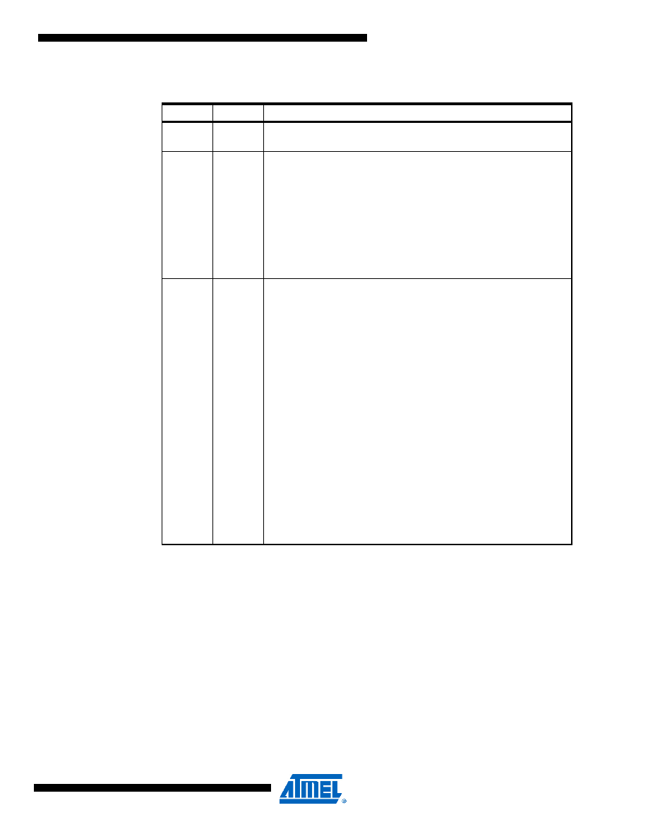
Table 20-1.
Relations between USIWM1..0 and the USI Operation
USIWM1
USIWM0
Description
0
Outputs, clock hold, and start detector disabled. Port pins operates as
normal.
0
1
Three-wire mode. Uses DO, DI, and USCK pins.
The Data Output (DO) pin overrides the corresponding bit in the PORT
Register in this mode. However, the corresponding DDR bit still
controls the data direction. When the port pin is set as input the pins
pull-up is controlled by the PORT bit.
The Data Input (DI) and Serial Clock (USCK) pins do not affect the
normal port operation. When operating as master, clock pulses are
software generated by toggling the PORT Register, while the data
direction is set to output. The USITC bit in the USICR Register can be
used for this purpose.
1
0
Two-wire mode. Uses SDA (DI) and SCL (USCK) pins(1).
The Serial Data (SDA) and the Serial Clock (SCL) pins are bi-
directional and uses open-collector output drives. The output drivers
are enabled by setting the corresponding bit for SDA and SCL in the
DDR Register.
When the output driver is enabled for the SDA pin, the output driver will
force the line SDA low if the output of the Shift Register or the
corresponding bit in the PORT Register is zero. Otherwise the SDA
line will not be driven (i.e., it is released). When the SCL pin output
driver is enabled the SCL line will be forced low if the corresponding bit
in the PORT Register is zero, or by the start detector. Otherwise the
SCL line will not be driven.
The SCL line is held low when a start detector detects a start condition
and the output is enabled. Clearing the Start Condition Flag (USISIF)
releases the line. The SDA and SCL pin inputs is not affected by
enabling this mode. Pull-ups on the SDA and SCL port pin are
disabled in Two-wire mode.
1
Two-wire mode. Uses SDA and SCL pins.
Same operation as for the Two-wire mode described above, except
that the SCL line is also held low when a counter overflow occurs, and
is held low until the Counter Overflow Flag (USIOIF) is cleared.
相关PDF资料 |
PDF描述 |
|---|---|
| D38999/20FJ7SN | CONN RCPT 99POS WALL MNT W/SCKT |
| PIC16LF723AT-I/MV | MCU 8BIT 4K FLASH XLP 28-UQFN |
| PIC16F723AT-I/MV | MCU 8BIT 4K FLASH XLP 28-UQFN |
| D38999/26WJ7SA | CONN PLUG 99POS STRAIGHT W/SCKT |
| PIC16LF1826T-I/SO | MCU 8BIT 2K FLASH 18SOIC |
相关代理商/技术参数 |
参数描述 |
|---|---|
| PIC16LF1824-I/ML | 功能描述:8位微控制器 -MCU 7KB Flash 256B RAM 32 MHz Int Osc Core RoHS:否 制造商:Silicon Labs 核心:8051 处理器系列:C8051F39x 数据总线宽度:8 bit 最大时钟频率:50 MHz 程序存储器大小:16 KB 数据 RAM 大小:1 KB 片上 ADC:Yes 工作电源电压:1.8 V to 3.6 V 工作温度范围:- 40 C to + 105 C 封装 / 箱体:QFN-20 安装风格:SMD/SMT |
| PIC16LF1824-I/P | 功能描述:8位微控制器 -MCU 7KB Flash 256B RAM 32 MHz Int Osc Core RoHS:否 制造商:Silicon Labs 核心:8051 处理器系列:C8051F39x 数据总线宽度:8 bit 最大时钟频率:50 MHz 程序存储器大小:16 KB 数据 RAM 大小:1 KB 片上 ADC:Yes 工作电源电压:1.8 V to 3.6 V 工作温度范围:- 40 C to + 105 C 封装 / 箱体:QFN-20 安装风格:SMD/SMT |
| PIC16LF1824-I/SL | 功能描述:8位微控制器 -MCU 7KB Flash 256B RAM 32 MHz Int Osc Core RoHS:否 制造商:Silicon Labs 核心:8051 处理器系列:C8051F39x 数据总线宽度:8 bit 最大时钟频率:50 MHz 程序存储器大小:16 KB 数据 RAM 大小:1 KB 片上 ADC:Yes 工作电源电压:1.8 V to 3.6 V 工作温度范围:- 40 C to + 105 C 封装 / 箱体:QFN-20 安装风格:SMD/SMT |
| PIC16LF1824-I/ST | 功能描述:8位微控制器 -MCU 7KB Flash 256B RAM 32 MHz Int Osc Core RoHS:否 制造商:Silicon Labs 核心:8051 处理器系列:C8051F39x 数据总线宽度:8 bit 最大时钟频率:50 MHz 程序存储器大小:16 KB 数据 RAM 大小:1 KB 片上 ADC:Yes 工作电源电压:1.8 V to 3.6 V 工作温度范围:- 40 C to + 105 C 封装 / 箱体:QFN-20 安装风格:SMD/SMT |
| PIC16LF1824T39A-I/ST | 制造商:Microchip Technology 功能描述:MCU 8-bit PIC16 PIC RISC 7KB Flash 2.5V/3.3V 20-Pin TSSOP 制造商:Microchip Technology Inc 功能描述:PIC16LF1824 MICROCONTROLLER WITH 300-900 MHZ TRANSMITTER - Rail/Tube 制造商:Microchip Technology Inc 功能描述:IC MCU 8BIT FLASH 20TSSOP 制造商:Microchip Technology Inc 功能描述:PIC16LF1824 Microcontroller |
发布紧急采购,3分钟左右您将得到回复。