- 您现在的位置:买卖IC网 > PDF目录10852 > PIC17C42AT-25I/L (Microchip Technology)IC MCU OTP 2KX16 PWM 44PLCC PDF资料下载
参数资料
| 型号: | PIC17C42AT-25I/L |
| 厂商: | Microchip Technology |
| 文件页数: | 191/241页 |
| 文件大小: | 0K |
| 描述: | IC MCU OTP 2KX16 PWM 44PLCC |
| 标准包装: | 500 |
| 系列: | PIC® 17C |
| 核心处理器: | PIC |
| 芯体尺寸: | 8-位 |
| 速度: | 25MHz |
| 连通性: | UART/USART |
| 外围设备: | POR,PWM,WDT |
| 输入/输出数: | 33 |
| 程序存储器容量: | 4KB(2K x 16) |
| 程序存储器类型: | OTP |
| RAM 容量: | 232 x 8 |
| 电压 - 电源 (Vcc/Vdd): | 4.5 V ~ 6 V |
| 振荡器型: | 外部 |
| 工作温度: | -40°C ~ 85°C |
| 封装/外壳: | 44-LCC(J 形引线) |
| 包装: | 带卷 (TR) |
| 配用: | AC164317-ND - MODULE SKT MPLAB PM3 44PLCC DVA17XL441-ND - DEVICE ADAPTER FOR PIC17C42A |
第1页第2页第3页第4页第5页第6页第7页第8页第9页第10页第11页第12页第13页第14页第15页第16页第17页第18页第19页第20页第21页第22页第23页第24页第25页第26页第27页第28页第29页第30页第31页第32页第33页第34页第35页第36页第37页第38页第39页第40页第41页第42页第43页第44页第45页第46页第47页第48页第49页第50页第51页第52页第53页第54页第55页第56页第57页第58页第59页第60页第61页第62页第63页第64页第65页第66页第67页第68页第69页第70页第71页第72页第73页第74页第75页第76页第77页第78页第79页第80页第81页第82页第83页第84页第85页第86页第87页第88页第89页第90页第91页第92页第93页第94页第95页第96页第97页第98页第99页第100页第101页第102页第103页第104页第105页第106页第107页第108页第109页第110页第111页第112页第113页第114页第115页第116页第117页第118页第119页第120页第121页第122页第123页第124页第125页第126页第127页第128页第129页第130页第131页第132页第133页第134页第135页第136页第137页第138页第139页第140页第141页第142页第143页第144页第145页第146页第147页第148页第149页第150页第151页第152页第153页第154页第155页第156页第157页第158页第159页第160页第161页第162页第163页第164页第165页第166页第167页第168页第169页第170页第171页第172页第173页第174页第175页第176页第177页第178页第179页第180页第181页第182页第183页第184页第185页第186页第187页第188页第189页第190页当前第191页第192页第193页第194页第195页第196页第197页第198页第199页第200页第201页第202页第203页第204页第205页第206页第207页第208页第209页第210页第211页第212页第213页第214页第215页第216页第217页第218页第219页第220页第221页第222页第223页第224页第225页第226页第227页第228页第229页第230页第231页第232页第233页第234页第235页第236页第237页第238页第239页第240页第241页
1996 Microchip Technology Inc.
DS30412C-page 53
PIC17C4X
9.0
I/O PORTS
The PIC17C4X devices have five I/O ports, PORTA
through PORTE. PORTB through PORTE have a corre-
sponding Data Direction Register (DDR), which is used
to congure the port pins as inputs or outputs. These
ve ports are made up of 33 I/O pins. Some of these
ports pins are multiplexed with alternate functions.
PORTC, PORTD, and PORTE are multiplexed with the
system bus. These pins are congured as the system
bus when the device’s conguration bits are selected to
Microprocessor or Extended Microcontroller modes. In
the two other microcontroller modes, these pins are
general purpose I/O.
PORTA and PORTB are multiplexed with the peripheral
features of the device. These peripheral features are:
Timer modules
Capture module
PWM module
USART/SCI module
External Interrupt pin
When some of these peripheral modules are turned on,
the port pin will automatically congure to the alternate
function. The modules that do this are:
PWM module
USART/SCI module
When a pin is automatically congured as an output by
a peripheral module, the pins data direction (DDR) bit
is unknown. After disabling the peripheral module, the
user should re-initialize the DDR bit to the desired con-
guration.
The other peripheral modules (which require an input)
must have their data direction bit congured appropri-
ately.
Note:
A pin that is a peripheral input, can be con-
gured as an output (DDRx<y> is cleared).
The peripheral events will be determined
by the action output on the port pin.
9.1
PORTA Register
PORTA is a 6-bit wide latch. PORTA does not have a
corresponding Data Direction Register (DDR).
Reading PORTA reads the status of the pins.
The RA1 pin is multiplexed with TMR0 clock input, and
RA4 and RA5 are multiplexed with the USART func-
tions. The control of RA4 and RA5 as outputs is auto-
matically congured by the USART module.
9.1.1
USING RA2, RA3 AS OUTPUTS
The RA2 and RA3 pins are open drain outputs. To use
the RA2 or the RA3 pin(s) as output(s), simply write to
the PORTA register the desired value. A '0' will cause
the pin to drive low, while a '1' will cause the pin to oat
(hi-impedance). An external pull-up resistor should be
used to pull the pin high. Writes to PORTA will not affect
the other pins.
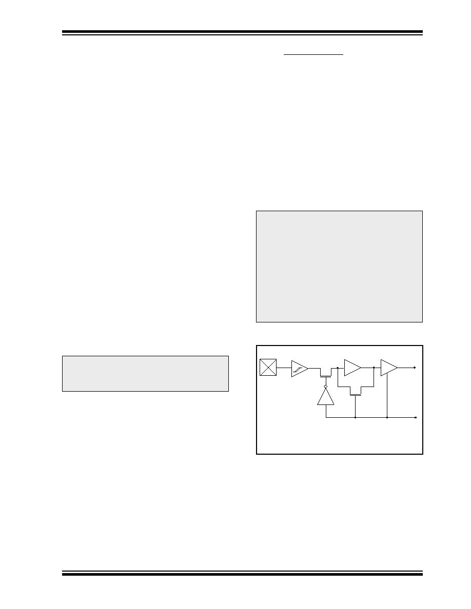
FIGURE 9-1:
RA0 AND RA1 BLOCK
DIAGRAM
Note:
When using the RA2 or RA3 pin(s) as out-
put(s), read-modify-write instructions (such
as BCF, BSF, BTG) on PORTA are not rec-
ommended.
Such operations read the port pins, do the
desired operation, and then write this value
to the data latch. This may inadvertently
cause the RA2 or RA3 pins to switch from
input to output (or vice-versa).
It is recommended to use a shadow regis-
ter for PORTA. Do the bit operations on this
shadow register and then move it to
PORTA.
Note: I/O pins have protection diodes to VDD and VSS.
DATA BUS
RD_PORTA
(Q2)
This document was created with FrameMaker404
相关PDF资料 |
PDF描述 |
|---|---|
| PIC17C42AT-25E/PT | IC MCU OTP 2KX16 PWM 44TQFP |
| PIC17C42AT-25E/PQ | IC MCU OTP 2KX16 PWM 44-MQFP |
| PIC17C42AT-25E/L | IC MCU OTP 2KX16 PWM 44PLCC |
| PIC17C42AT-16/PQ | IC MCU OTP 2KX16 PWM 44-MQFP |
| PIC17C42AT-16/L | IC MCU OTP 2KX16 PWM 44PLCC |
相关代理商/技术参数 |
参数描述 |
|---|---|
| PIC17C42AT-33/L | 功能描述:8位微控制器 -MCU 4KB 232 RAM 33 I/O RoHS:否 制造商:Silicon Labs 核心:8051 处理器系列:C8051F39x 数据总线宽度:8 bit 最大时钟频率:50 MHz 程序存储器大小:16 KB 数据 RAM 大小:1 KB 片上 ADC:Yes 工作电源电压:1.8 V to 3.6 V 工作温度范围:- 40 C to + 105 C 封装 / 箱体:QFN-20 安装风格:SMD/SMT |
| PIC17C42AT-33/PQ | 功能描述:8位微控制器 -MCU 4KB 232 RAM 33 I/O RoHS:否 制造商:Silicon Labs 核心:8051 处理器系列:C8051F39x 数据总线宽度:8 bit 最大时钟频率:50 MHz 程序存储器大小:16 KB 数据 RAM 大小:1 KB 片上 ADC:Yes 工作电源电压:1.8 V to 3.6 V 工作温度范围:- 40 C to + 105 C 封装 / 箱体:QFN-20 安装风格:SMD/SMT |
| PIC17C42AT-33/PT | 功能描述:8位微控制器 -MCU 4KB 232 RAM 33 I/O RoHS:否 制造商:Silicon Labs 核心:8051 处理器系列:C8051F39x 数据总线宽度:8 bit 最大时钟频率:50 MHz 程序存储器大小:16 KB 数据 RAM 大小:1 KB 片上 ADC:Yes 工作电源电压:1.8 V to 3.6 V 工作温度范围:- 40 C to + 105 C 封装 / 箱体:QFN-20 安装风格:SMD/SMT |
| PIC17C42AT-33E/L | 功能描述:8位微控制器 -MCU 4KB 232 RAM 33 I/O RoHS:否 制造商:Silicon Labs 核心:8051 处理器系列:C8051F39x 数据总线宽度:8 bit 最大时钟频率:50 MHz 程序存储器大小:16 KB 数据 RAM 大小:1 KB 片上 ADC:Yes 工作电源电压:1.8 V to 3.6 V 工作温度范围:- 40 C to + 105 C 封装 / 箱体:QFN-20 安装风格:SMD/SMT |
| PIC17C42AT-33E/PQ | 功能描述:8位微控制器 -MCU 4KB 232 RAM 33 I/O RoHS:否 制造商:Silicon Labs 核心:8051 处理器系列:C8051F39x 数据总线宽度:8 bit 最大时钟频率:50 MHz 程序存储器大小:16 KB 数据 RAM 大小:1 KB 片上 ADC:Yes 工作电源电压:1.8 V to 3.6 V 工作温度范围:- 40 C to + 105 C 封装 / 箱体:QFN-20 安装风格:SMD/SMT |
发布紧急采购,3分钟左右您将得到回复。