- 您现在的位置:买卖IC网 > PDF目录10852 > PIC17C42AT-25I/L (Microchip Technology)IC MCU OTP 2KX16 PWM 44PLCC PDF资料下载
参数资料
| 型号: | PIC17C42AT-25I/L |
| 厂商: | Microchip Technology |
| 文件页数: | 214/241页 |
| 文件大小: | 0K |
| 描述: | IC MCU OTP 2KX16 PWM 44PLCC |
| 标准包装: | 500 |
| 系列: | PIC® 17C |
| 核心处理器: | PIC |
| 芯体尺寸: | 8-位 |
| 速度: | 25MHz |
| 连通性: | UART/USART |
| 外围设备: | POR,PWM,WDT |
| 输入/输出数: | 33 |
| 程序存储器容量: | 4KB(2K x 16) |
| 程序存储器类型: | OTP |
| RAM 容量: | 232 x 8 |
| 电压 - 电源 (Vcc/Vdd): | 4.5 V ~ 6 V |
| 振荡器型: | 外部 |
| 工作温度: | -40°C ~ 85°C |
| 封装/外壳: | 44-LCC(J 形引线) |
| 包装: | 带卷 (TR) |
| 配用: | AC164317-ND - MODULE SKT MPLAB PM3 44PLCC DVA17XL441-ND - DEVICE ADAPTER FOR PIC17C42A |
第1页第2页第3页第4页第5页第6页第7页第8页第9页第10页第11页第12页第13页第14页第15页第16页第17页第18页第19页第20页第21页第22页第23页第24页第25页第26页第27页第28页第29页第30页第31页第32页第33页第34页第35页第36页第37页第38页第39页第40页第41页第42页第43页第44页第45页第46页第47页第48页第49页第50页第51页第52页第53页第54页第55页第56页第57页第58页第59页第60页第61页第62页第63页第64页第65页第66页第67页第68页第69页第70页第71页第72页第73页第74页第75页第76页第77页第78页第79页第80页第81页第82页第83页第84页第85页第86页第87页第88页第89页第90页第91页第92页第93页第94页第95页第96页第97页第98页第99页第100页第101页第102页第103页第104页第105页第106页第107页第108页第109页第110页第111页第112页第113页第114页第115页第116页第117页第118页第119页第120页第121页第122页第123页第124页第125页第126页第127页第128页第129页第130页第131页第132页第133页第134页第135页第136页第137页第138页第139页第140页第141页第142页第143页第144页第145页第146页第147页第148页第149页第150页第151页第152页第153页第154页第155页第156页第157页第158页第159页第160页第161页第162页第163页第164页第165页第166页第167页第168页第169页第170页第171页第172页第173页第174页第175页第176页第177页第178页第179页第180页第181页第182页第183页第184页第185页第186页第187页第188页第189页第190页第191页第192页第193页第194页第195页第196页第197页第198页第199页第200页第201页第202页第203页第204页第205页第206页第207页第208页第209页第210页第211页第212页第213页当前第214页第215页第216页第217页第218页第219页第220页第221页第222页第223页第224页第225页第226页第227页第228页第229页第230页第231页第232页第233页第234页第235页第236页第237页第238页第239页第240页第241页
PIC17C4X
DS30412C-page 74
1996 Microchip Technology Inc.
12.1.2
TIMER1 & TIMER2 IN 16-BIT MODE
To select 16-bit mode, the T16 bit must be set. In this
mode TMR1 and TMR2 are concatenated to form a
16-bit timer (TMR2:TMR1). The 16-bit timer incre-
ments until it matches the 16-bit period register
(PR2:PR1). On the following timer clock, the timer
value is reset to 0h, and the TMR1IF bit is set.
When selecting the clock source for the16-bit timer, the
TMR1CS bit controls the entire 16-bit timer and
TMR2CS is a “don’t care.” When TMR1CS is clear, the
timer increments once every instruction cycle (Fosc/4).
When TMR1CS is set, the timer increments on every
falling edge of the RB4/TCLK12 pin. For the 16-bit timer
to increment, both TMR1ON and TMR2ON bits must be
set (Table 12-1).
12.1.2.1
EXTERNAL CLOCK INPUT FOR
TMR1:TMR2
When TMR1CS is set, the 16-bit TMR2:TMR1 incre-
ments on the falling edge of clock input TCLK12. The
input on the RB4/TCLK12 pin is sampled and synchro-
nized by the internal phase clocks twice every instruc-
tion cycle. This causes a delay from the time a falling
edge
appears
on
RB4/TCLK12
to
the
time
TMR2:TMR1 is actually incremented. For the external
clock input timing requirements, see the Electrical
Specication section.
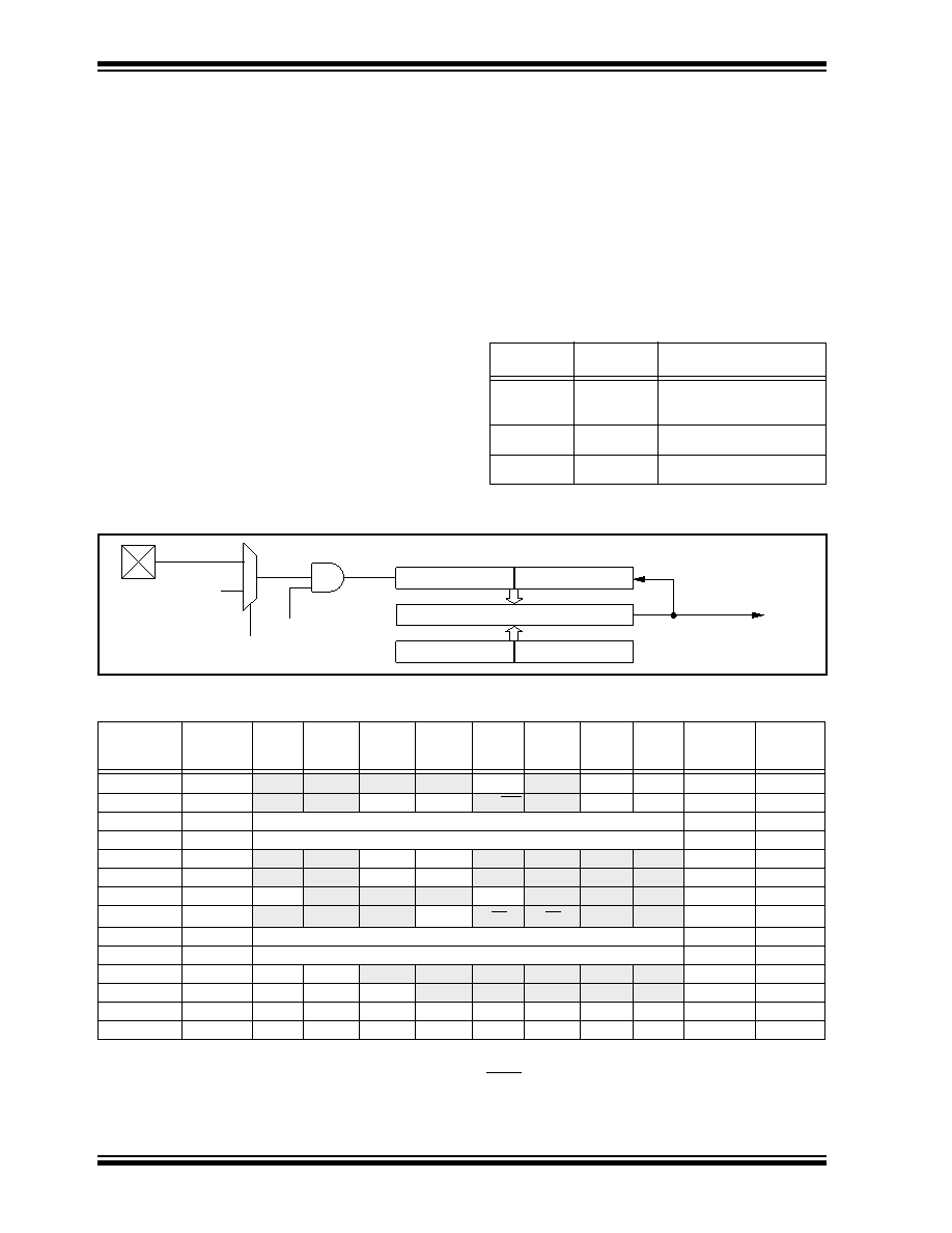
TABLE 12-1:
TURNING ON 16-BIT TIMER
TMR2ON
TMR1ON
Result
11
16-bit timer
(TMR2:TMR1) ON
01
Only TMR1 increments
x0
16-bit timer OFF
FIGURE 12-4: TMR1 AND TMR2 IN 16-BIT TIMER/COUNTER MODE
TABLE 12-2:
SUMMARY OF TIMER1 AND TIMER2 REGISTERS
Address
Name
Bit 7
Bit 6
Bit 5
Bit 4
Bit 3
Bit 2
Bit 1
Bit 0
Value on
Power-on
Reset
Value on all
other resets
(Note1)
16h, Bank 3
TCON1
CA2ED1
CA2ED0
CA1ED1
CA1ED0
T16
TMR3CS TMR2CS TMR1CS 0000 0000
0000 0000
17h, Bank 3
TCON2
CA2OVF
CA1OVF PWM2ON PWM1ON CA1/PR3 TMR3ON TMR2ON TMR1ON 0000 0000
0000 0000
10h, Bank 2
TMR1
Timer1 register
xxxx xxxx
uuuu uuuu
11h, Bank 2
TMR2
Timer2 register
xxxx xxxx
uuuu uuuu
16h, Bank 1
PIR
RBIF
TMR3IF
TMR2IF
TMR1IF
CA2IF
CA1IF
TXIF
RCIF
0000 0010
17h, Bank 1
PIE
RBIE
TMR3IE
TMR2IE
TMR1IE
CA2IE
CA1IE
TXIE
RCIE
0000 0000
07h, Unbanked
INTSTA
PEIF
T0CKIF
T0IF
INTF
PEIE
T0CKIE
T0IE
INTE
0000 0000
06h, Unbanked
CPUSTA
—
STKAV
GLINTD
TO
PD
—
--11 11--
--11 qq--
14h, Bank 2
PR1
Timer1 period register
xxxx xxxx
uuuu uuuu
15h, Bank 2
PR2
Timer2 period register
xxxx xxxx
uuuu uuuu
10h, Bank 3
PW1DCL
DC1
DC0
—
xx-- ----
uu-- ----
11h, Bank 3
PW2DCL
DC1
DC0
TM2PW2
—
xx0- ----
uu0- ----
12h, Bank 3
PW1DCH
DC9
DC8
DC7
DC6
DC5
DC4
DC3
DC2
xxxx xxxx
uuuu uuuu
13h, Bank 3
PW2DCH
DC9
DC8
DC7
DC6
DC5
DC4
DC3
DC2
xxxx xxxx
uuuu uuuu
Legend: x = unknown, u = unchanged, - = unimplemented read as a '0', q - value depends on condition,
shaded cells are not used by Timer1 or Timer2.
Note 1:
Other (non power-up) resets include: external reset through MCLR and WDT Timer Reset.
RB4/TCLK12
Fosc/4
TMR1ON
(TCON2<0>)
TMR1CS
(TCON1<0>)
TMR1 x 8
PR1 x 8
Reset
Equal
Set Interrupt TMR1IF
(PIR<4>)
1
0
Comparator<8>
Comparator x16
TMR2 x 8
PR2 x 8
相关PDF资料 |
PDF描述 |
|---|---|
| PIC17C42AT-25E/PT | IC MCU OTP 2KX16 PWM 44TQFP |
| PIC17C42AT-25E/PQ | IC MCU OTP 2KX16 PWM 44-MQFP |
| PIC17C42AT-25E/L | IC MCU OTP 2KX16 PWM 44PLCC |
| PIC17C42AT-16/PQ | IC MCU OTP 2KX16 PWM 44-MQFP |
| PIC17C42AT-16/L | IC MCU OTP 2KX16 PWM 44PLCC |
相关代理商/技术参数 |
参数描述 |
|---|---|
| PIC17C42AT-33/L | 功能描述:8位微控制器 -MCU 4KB 232 RAM 33 I/O RoHS:否 制造商:Silicon Labs 核心:8051 处理器系列:C8051F39x 数据总线宽度:8 bit 最大时钟频率:50 MHz 程序存储器大小:16 KB 数据 RAM 大小:1 KB 片上 ADC:Yes 工作电源电压:1.8 V to 3.6 V 工作温度范围:- 40 C to + 105 C 封装 / 箱体:QFN-20 安装风格:SMD/SMT |
| PIC17C42AT-33/PQ | 功能描述:8位微控制器 -MCU 4KB 232 RAM 33 I/O RoHS:否 制造商:Silicon Labs 核心:8051 处理器系列:C8051F39x 数据总线宽度:8 bit 最大时钟频率:50 MHz 程序存储器大小:16 KB 数据 RAM 大小:1 KB 片上 ADC:Yes 工作电源电压:1.8 V to 3.6 V 工作温度范围:- 40 C to + 105 C 封装 / 箱体:QFN-20 安装风格:SMD/SMT |
| PIC17C42AT-33/PT | 功能描述:8位微控制器 -MCU 4KB 232 RAM 33 I/O RoHS:否 制造商:Silicon Labs 核心:8051 处理器系列:C8051F39x 数据总线宽度:8 bit 最大时钟频率:50 MHz 程序存储器大小:16 KB 数据 RAM 大小:1 KB 片上 ADC:Yes 工作电源电压:1.8 V to 3.6 V 工作温度范围:- 40 C to + 105 C 封装 / 箱体:QFN-20 安装风格:SMD/SMT |
| PIC17C42AT-33E/L | 功能描述:8位微控制器 -MCU 4KB 232 RAM 33 I/O RoHS:否 制造商:Silicon Labs 核心:8051 处理器系列:C8051F39x 数据总线宽度:8 bit 最大时钟频率:50 MHz 程序存储器大小:16 KB 数据 RAM 大小:1 KB 片上 ADC:Yes 工作电源电压:1.8 V to 3.6 V 工作温度范围:- 40 C to + 105 C 封装 / 箱体:QFN-20 安装风格:SMD/SMT |
| PIC17C42AT-33E/PQ | 功能描述:8位微控制器 -MCU 4KB 232 RAM 33 I/O RoHS:否 制造商:Silicon Labs 核心:8051 处理器系列:C8051F39x 数据总线宽度:8 bit 最大时钟频率:50 MHz 程序存储器大小:16 KB 数据 RAM 大小:1 KB 片上 ADC:Yes 工作电源电压:1.8 V to 3.6 V 工作温度范围:- 40 C to + 105 C 封装 / 箱体:QFN-20 安装风格:SMD/SMT |
发布紧急采购,3分钟左右您将得到回复。