- 您现在的位置:买卖IC网 > PDF目录10852 > PIC17C42AT-25I/L (Microchip Technology)IC MCU OTP 2KX16 PWM 44PLCC PDF资料下载
参数资料
| 型号: | PIC17C42AT-25I/L |
| 厂商: | Microchip Technology |
| 文件页数: | 216/241页 |
| 文件大小: | 0K |
| 描述: | IC MCU OTP 2KX16 PWM 44PLCC |
| 标准包装: | 500 |
| 系列: | PIC® 17C |
| 核心处理器: | PIC |
| 芯体尺寸: | 8-位 |
| 速度: | 25MHz |
| 连通性: | UART/USART |
| 外围设备: | POR,PWM,WDT |
| 输入/输出数: | 33 |
| 程序存储器容量: | 4KB(2K x 16) |
| 程序存储器类型: | OTP |
| RAM 容量: | 232 x 8 |
| 电压 - 电源 (Vcc/Vdd): | 4.5 V ~ 6 V |
| 振荡器型: | 外部 |
| 工作温度: | -40°C ~ 85°C |
| 封装/外壳: | 44-LCC(J 形引线) |
| 包装: | 带卷 (TR) |
| 配用: | AC164317-ND - MODULE SKT MPLAB PM3 44PLCC DVA17XL441-ND - DEVICE ADAPTER FOR PIC17C42A |
第1页第2页第3页第4页第5页第6页第7页第8页第9页第10页第11页第12页第13页第14页第15页第16页第17页第18页第19页第20页第21页第22页第23页第24页第25页第26页第27页第28页第29页第30页第31页第32页第33页第34页第35页第36页第37页第38页第39页第40页第41页第42页第43页第44页第45页第46页第47页第48页第49页第50页第51页第52页第53页第54页第55页第56页第57页第58页第59页第60页第61页第62页第63页第64页第65页第66页第67页第68页第69页第70页第71页第72页第73页第74页第75页第76页第77页第78页第79页第80页第81页第82页第83页第84页第85页第86页第87页第88页第89页第90页第91页第92页第93页第94页第95页第96页第97页第98页第99页第100页第101页第102页第103页第104页第105页第106页第107页第108页第109页第110页第111页第112页第113页第114页第115页第116页第117页第118页第119页第120页第121页第122页第123页第124页第125页第126页第127页第128页第129页第130页第131页第132页第133页第134页第135页第136页第137页第138页第139页第140页第141页第142页第143页第144页第145页第146页第147页第148页第149页第150页第151页第152页第153页第154页第155页第156页第157页第158页第159页第160页第161页第162页第163页第164页第165页第166页第167页第168页第169页第170页第171页第172页第173页第174页第175页第176页第177页第178页第179页第180页第181页第182页第183页第184页第185页第186页第187页第188页第189页第190页第191页第192页第193页第194页第195页第196页第197页第198页第199页第200页第201页第202页第203页第204页第205页第206页第207页第208页第209页第210页第211页第212页第213页第214页第215页当前第216页第217页第218页第219页第220页第221页第222页第223页第224页第225页第226页第227页第228页第229页第230页第231页第232页第233页第234页第235页第236页第237页第238页第239页第240页第241页
PIC17C4X
DS30412C-page 76
1996 Microchip Technology Inc.
12.1.3.1
PWM PERIODS
The period of the PWM1 output is determined by
Timer1 and its period register (PR1). The period of the
PWM2 output can be software congured to use either
Timer1 or Timer2 as the time-base. When TM2PW2 bit
(PW2DCL<5>) is clear, the time-base is determined by
TMR1 and PR1. When TM2PW2 is set, the time-base
is determined by Timer2 and PR2.
Running two different PWM outputs on two different
timers allows different PWM periods. Running both
PWMs from Timer1 allows the best use of resources by
freeing Timer2 to operate as an 8-bit timer. Timer1 and
Timer2 can not be used as a 16-bit timer if either PWM
is being used.
The PWM periods can be calculated as follows:
period of PWM1 =[(PR1) + 1] x 4TOSC
period of PWM2 =[(PR1) + 1] x 4TOSC or
[(PR2) + 1] x 4TOSC
The duty cycle of PWMx is determined by the 10-bit
value DCx<9:0>. The upper 8-bits are from register
PWxDCH and the lower 2-bits are from PWxDCL<7:6>
(PWxDCH:PWxDCL<7:6>).
shows
the
maximum PWM frequency (FPWM) given the value in
the period register.
The number of bits of resolution that the PWM can
achieve depends on the operation frequency of the
device as well as the PWM frequency (FPWM).
Maximum PWM resolution (bits) for a given PWM fre-
quency:
The PWMx duty cycle is as follows:
PWMx Duty Cycle =
(DCx) x TOSC
where
DCx
represents
the
10-bit
value
from
PWxDCH:PWxDCL.
If DCx = 0, then the duty cycle is zero. If PRx =
PWxDCH, then the PWM output will be low for one to
four
Q-clock
(depending
on
the
state
of
the
PWxDCL<7:6> bits). For a Duty Cycle to be 100%, the
PWxDCH value must be greater then the PRx value.
The duty cycle registers for both PWM outputs are dou-
ble buffered. When the user writes to these registers,
they are stored in master latches. When TMR1 (or
TMR2) overows and a new PWM period begins, the
master latch values are transferred to the slave latches
and the PWMx pin is forced high.
Note:
For PW1DCH, PW1DCL, PW2DCH and
PW2DCL registers, a write operation
writes to the "master latches" while a read
operation reads the "slave latches". As a
result, the user may not read back what
was just written to the duty cycle registers.
log
(
FPWM
log (2)
FOSC
)
bits
=
The user should also avoid any "read-modify-write"
operations on the duty cycle registers, such as: ADDWF
PW1DCH
. This may cause duty cycle outputs that are
unpredictable.
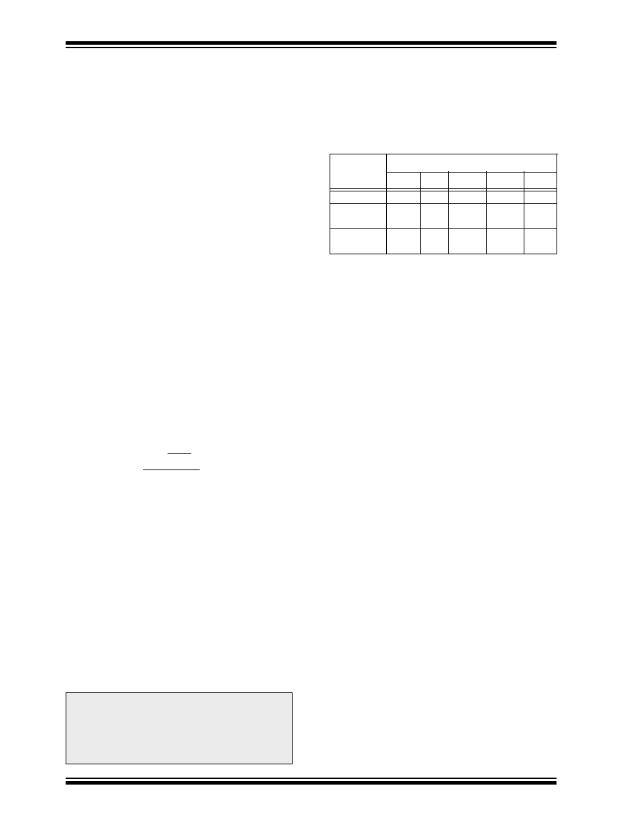
TABLE 12-3:
PWM FREQUENCY vs.
RESOLUTION AT 25 MHz
12.1.3.2
PWM INTERRUPTS
The PWM module makes use of TMR1 or TMR2 inter-
rupts. A timer interrupt is generated when TMR1 or
TMR2 equals its period register and is cleared to zero.
This interrupt also marks the beginning of a PWM
cycle. The user can write new duty cycle values before
the timer roll-over. The TMR1 interrupt is latched into
the TMR1IF bit and the TMR2 interrupt is latched into
the TMR2IF bit. These ags must be cleared in soft-
ware.
12.1.3.3
EXTERNAL CLOCK SOURCE
The PWMs will operate regardless of the clock source
of the timer. The use of an external clock has ramica-
tions that must be understood. Because the external
TCLK12 input is synchronized internally (sampled once
per instruction cycle), the time TCLK12 changes to the
time the timer increments will vary by as much as TCY
(one instruction cycle). This will cause jitter in the duty
cycle as well as the period of the PWM output.
This jitter will be
±TCY, unless the external clock is syn-
chronized with the processor clock. Use of one of the
PWM outputs as the clock source to the TCLKx input,
will supply a synchronized clock.
In general, when using an external clock source for
PWM, its frequency should be much less than the
device frequency (Fosc).
PWM
Frequency
Frequency (kHz)
24.4
48.8
65.104
97.66
390.6
PRx Value
0xFF
0x7F 0x5F
0x3F
0x0F
High
Resolution
10-bit
9-bit
8.5-bit
8-bit
6-bit
Standard
Resolution
8-bit
7-bit
6.5-bit
6-bit
4-bit
相关PDF资料 |
PDF描述 |
|---|---|
| PIC17C42AT-25E/PT | IC MCU OTP 2KX16 PWM 44TQFP |
| PIC17C42AT-25E/PQ | IC MCU OTP 2KX16 PWM 44-MQFP |
| PIC17C42AT-25E/L | IC MCU OTP 2KX16 PWM 44PLCC |
| PIC17C42AT-16/PQ | IC MCU OTP 2KX16 PWM 44-MQFP |
| PIC17C42AT-16/L | IC MCU OTP 2KX16 PWM 44PLCC |
相关代理商/技术参数 |
参数描述 |
|---|---|
| PIC17C42AT-33/L | 功能描述:8位微控制器 -MCU 4KB 232 RAM 33 I/O RoHS:否 制造商:Silicon Labs 核心:8051 处理器系列:C8051F39x 数据总线宽度:8 bit 最大时钟频率:50 MHz 程序存储器大小:16 KB 数据 RAM 大小:1 KB 片上 ADC:Yes 工作电源电压:1.8 V to 3.6 V 工作温度范围:- 40 C to + 105 C 封装 / 箱体:QFN-20 安装风格:SMD/SMT |
| PIC17C42AT-33/PQ | 功能描述:8位微控制器 -MCU 4KB 232 RAM 33 I/O RoHS:否 制造商:Silicon Labs 核心:8051 处理器系列:C8051F39x 数据总线宽度:8 bit 最大时钟频率:50 MHz 程序存储器大小:16 KB 数据 RAM 大小:1 KB 片上 ADC:Yes 工作电源电压:1.8 V to 3.6 V 工作温度范围:- 40 C to + 105 C 封装 / 箱体:QFN-20 安装风格:SMD/SMT |
| PIC17C42AT-33/PT | 功能描述:8位微控制器 -MCU 4KB 232 RAM 33 I/O RoHS:否 制造商:Silicon Labs 核心:8051 处理器系列:C8051F39x 数据总线宽度:8 bit 最大时钟频率:50 MHz 程序存储器大小:16 KB 数据 RAM 大小:1 KB 片上 ADC:Yes 工作电源电压:1.8 V to 3.6 V 工作温度范围:- 40 C to + 105 C 封装 / 箱体:QFN-20 安装风格:SMD/SMT |
| PIC17C42AT-33E/L | 功能描述:8位微控制器 -MCU 4KB 232 RAM 33 I/O RoHS:否 制造商:Silicon Labs 核心:8051 处理器系列:C8051F39x 数据总线宽度:8 bit 最大时钟频率:50 MHz 程序存储器大小:16 KB 数据 RAM 大小:1 KB 片上 ADC:Yes 工作电源电压:1.8 V to 3.6 V 工作温度范围:- 40 C to + 105 C 封装 / 箱体:QFN-20 安装风格:SMD/SMT |
| PIC17C42AT-33E/PQ | 功能描述:8位微控制器 -MCU 4KB 232 RAM 33 I/O RoHS:否 制造商:Silicon Labs 核心:8051 处理器系列:C8051F39x 数据总线宽度:8 bit 最大时钟频率:50 MHz 程序存储器大小:16 KB 数据 RAM 大小:1 KB 片上 ADC:Yes 工作电源电压:1.8 V to 3.6 V 工作温度范围:- 40 C to + 105 C 封装 / 箱体:QFN-20 安装风格:SMD/SMT |
发布紧急采购,3分钟左右您将得到回复。