- 您现在的位置:买卖IC网 > PDF目录11439 > PIC18F46J53T-I/ML (Microchip Technology)IC MCU 8BIT 64KB FLASH 44QFN PDF资料下载
参数资料
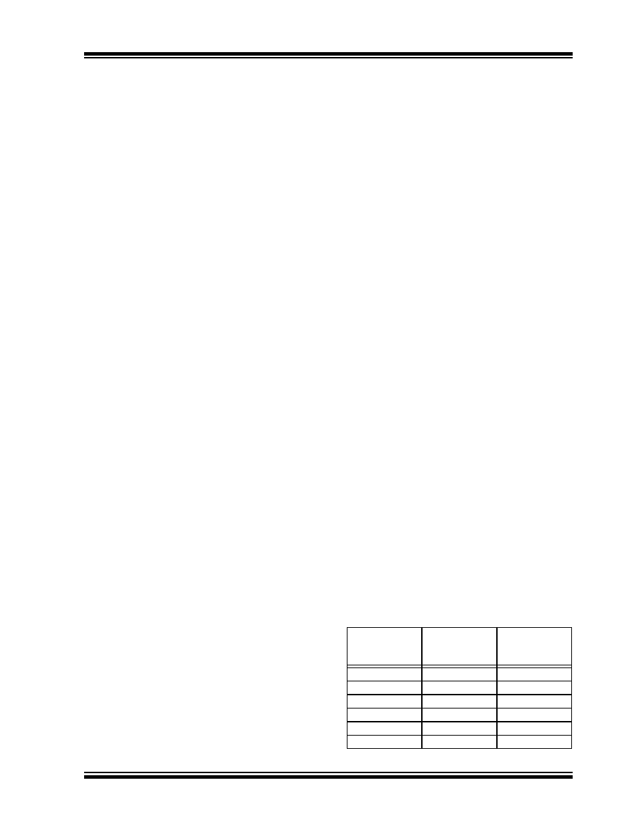
| 型号: | PIC18F46J53T-I/ML |
| 厂商: | Microchip Technology |
| 文件页数: | 183/389页 |
| 文件大小: | 0K |
| 描述: | IC MCU 8BIT 64KB FLASH 44QFN |
| 标准包装: | 1,600 |
| 系列: | PIC® XLP™ 18F |
| 核心处理器: | PIC |
| 芯体尺寸: | 8-位 |
| 速度: | 48MHz |
| 连通性: | I²C,LIN,SPI,UART/USART,USB |
| 外围设备: | 欠压检测/复位,POR,PWM,WDT |
| 输入/输出数: | 34 |
| 程序存储器容量: | 64KB(32K x 16) |
| 程序存储器类型: | 闪存 |
| RAM 容量: | 3.8K x 8 |
| 电压 - 电源 (Vcc/Vdd): | 2.15 V ~ 3.6 V |
| 数据转换器: | A/D 13x10b/12b |
| 振荡器型: | 内部 |
| 工作温度: | -40°C ~ 85°C |
| 封装/外壳: | 44-VQFN 裸露焊盘 |
| 包装: | 带卷 (TR) |
第1页第2页第3页第4页第5页第6页第7页第8页第9页第10页第11页第12页第13页第14页第15页第16页第17页第18页第19页第20页第21页第22页第23页第24页第25页第26页第27页第28页第29页第30页第31页第32页第33页第34页第35页第36页第37页第38页第39页第40页第41页第42页第43页第44页第45页第46页第47页第48页第49页第50页第51页第52页第53页第54页第55页第56页第57页第58页第59页第60页第61页第62页第63页第64页第65页第66页第67页第68页第69页第70页第71页第72页第73页第74页第75页第76页第77页第78页第79页第80页第81页第82页第83页第84页第85页第86页第87页第88页第89页第90页第91页第92页第93页第94页第95页第96页第97页第98页第99页第100页第101页第102页第103页第104页第105页第106页第107页第108页第109页第110页第111页第112页第113页第114页第115页第116页第117页第118页第119页第120页第121页第122页第123页第124页第125页第126页第127页第128页第129页第130页第131页第132页第133页第134页第135页第136页第137页第138页第139页第140页第141页第142页第143页第144页第145页第146页第147页第148页第149页第150页第151页第152页第153页第154页第155页第156页第157页第158页第159页第160页第161页第162页第163页第164页第165页第166页第167页第168页第169页第170页第171页第172页第173页第174页第175页第176页第177页第178页第179页第180页第181页第182页当前第183页第184页第185页第186页第187页第188页第189页第190页第191页第192页第193页第194页第195页第196页第197页第198页第199页第200页第201页第202页第203页第204页第205页第206页第207页第208页第209页第210页第211页第212页第213页第214页第215页第216页第217页第218页第219页第220页第221页第222页第223页第224页第225页第226页第227页第228页第229页第230页第231页第232页第233页第234页第235页第236页第237页第238页第239页第240页第241页第242页第243页第244页第245页第246页第247页第248页第249页第250页第251页第252页第253页第254页第255页第256页第257页第258页第259页第260页第261页第262页第263页第264页第265页第266页第267页第268页第269页第270页第271页第272页第273页第274页第275页第276页第277页第278页第279页第280页第281页第282页第283页第284页第285页第286页第287页第288页第289页第290页第291页第292页第293页第294页第295页第296页第297页第298页第299页第300页第301页第302页第303页第304页第305页第306页第307页第308页第309页第310页第311页第312页第313页第314页第315页第316页第317页第318页第319页第320页第321页第322页第323页第324页第325页第326页第327页第328页第329页第330页第331页第332页第333页第334页第335页第336页第337页第338页第339页第340页第341页第342页第343页第344页第345页第346页第347页第348页第349页第350页第351页第352页第353页第354页第355页第356页第357页第358页第359页第360页第361页第362页第363页第364页第365页第366页第367页第368页第369页第370页第371页第372页第373页第374页第375页第376页第377页第378页第379页第380页第381页第382页第383页第384页第385页第386页第387页第388页第389页
2010 Microchip Technology Inc.
DS39774D-page 279
PIC18F85J11 FAMILY
23.0 SPECIAL FEATURES OF THE
CPU
PIC18F85J11 family devices include several features
intended to maximize reliability and minimize cost
through elimination of external components. These are:
Oscillator Selection
Resets:
- Power-on Reset (POR)
- Power-up Timer (PWRT)
- Oscillator Start-up Timer (OST)
- Brown-out Reset (BOR)
Interrupts
Watchdog Timer (WDT)
Fail-Safe Clock Monitor
Two-Speed Start-up
Code Protection
In-Circuit Serial Programming
The oscillator can be configured for the application
depending on frequency, power, accuracy and cost. All
of the options are discussed in detail in Section 3.0
A complete discussion of device Resets and interrupts
is available in previous sections of this data sheet.
In addition to their Power-up and Oscillator Start-up
Timers provided for Resets, the PIC18F85J11 family of
devices have a configurable Watchdog Timer which is
controlled in software.
The inclusion of an internal RC oscillator also provides
the additional benefits of a Fail-Safe Clock Monitor
(FSCM) and Two-Speed Start-up. FSCM provides for
background monitoring of the peripheral clock and
automatic switchover in the event of its failure.
Two-Speed Start-up enables code to be executed
almost immediately on start-up while the primary clock
source completes its start-up delays.
All of these features are enabled and configured by
setting the appropriate Configuration register bits.
23.1
Configuration Bits
The Configuration bits can be programmed (read as
‘0’), or left unprogrammed (read as ‘1’), to select
various device configurations. These bits are mapped
starting at program memory location 300000h. A
complete list is shown in Table 23-2. A detailed
explanation of the various bit functions is provided in
Register 23-1 through Register 23-6.
23.1.1
CONSIDERATIONS FOR
CONFIGURING THE PIC18F85J11
FAMILY DEVICES
Unlike some previous PIC18 microcontrollers, devices
of the PIC18F85J11 family do not use persistent
memory registers to store configuration information.
The Configuration registers, CONFIG1L through
CONFIG4H, are implemented as volatile memory.
Immediately after power-up, or after a device Reset,
the microcontroller hardware automatically loads the
CONFIG1L through CONFIG4L registers with configu-
ration data stored in nonvolatile Flash program
memory. The last four words of Flash program memory,
known as the Flash Configuration Words (FCW), are
used to store the configuration data. Table 23-1
provides the Flash program memory, which will be
loaded into the corresponding Configuration register.
When creating applications for these devices, users
should always specifically allocate the location of the
Flash Configuration Word for configuration data. This is
to make certain that program code is not stored in this
address when the code is compiled.
The volatile memory cells used for the Configuration
bits always reset to ‘1’ on Power-on Resets. For all
other
types
of
Reset
events,
the
previously
programmed values are maintained and used without
reloading from program memory.
The four Most Significant bits of CONFIG1H,
CONFIG2H and CONFIG3H in program memory
should also be ‘1111’. This makes these Configuration
Words appear to be NOP instructions in the remote
event that their locations are ever executed by
accident. Since Configuration bits are not implemented
in the corresponding locations, writing ‘1’s to these
locations has no effect on device operation.
To prevent inadvertent configuration changes during
code execution, all programmable Configuration bits
are write-once. After a bit is initially programmed during
a power cycle, it cannot be written to again. Changing
a device configuration requires that power to the device
be cycled.
TABLE 23-1:
MAPPING OF THE FLASH
CONFIGURATION WORDS TO
THE CONFIGURATION
REGISTERS
Configuration
Byte
Code Space
Address
Configuration
Register
Address
CONFIG1L
XXXF8h
300000h
CONFIG1H
XXXF9h
300001h
CONFIG2L
XXXFAh
300002h
CONFIG2H
XXXFBh
300003h
CONFIG3L
XXXFCh
300004h
CONFIG3H
XXXFDh
300005h
相关PDF资料 |
PDF描述 |
|---|---|
| VE-J1Z-IW-B1 | CONVERTER MOD DC/DC 2V 40W |
| MC74HC4052ADTR2G | IC MUX/DEMUX DUAL 4X1 16TSSOP |
| VE-J1Y-IX-B1 | CONVERTER MOD DC/DC 3.3V 49.5W |
| VI-J1Z-IX-B1 | CONVERTER MOD DC/DC 2V 30W |
| PIC18F67J93-I/PT | IC PIC MCU FLASH 128KX4 64-TQFP |
相关代理商/技术参数 |
参数描述 |
|---|---|
| PIC18F46K20-E/ML | 功能描述:8位微控制器 -MCU 64KB Flash 3968B RAM 36 I/O 8B RoHS:否 制造商:Silicon Labs 核心:8051 处理器系列:C8051F39x 数据总线宽度:8 bit 最大时钟频率:50 MHz 程序存储器大小:16 KB 数据 RAM 大小:1 KB 片上 ADC:Yes 工作电源电压:1.8 V to 3.6 V 工作温度范围:- 40 C to + 105 C 封装 / 箱体:QFN-20 安装风格:SMD/SMT |
| PIC18F46K20-E/MV | 功能描述:8位微控制器 -MCU 64KB FL 3968b RAM 8b Familynanowatt XLP RoHS:否 制造商:Silicon Labs 核心:8051 处理器系列:C8051F39x 数据总线宽度:8 bit 最大时钟频率:50 MHz 程序存储器大小:16 KB 数据 RAM 大小:1 KB 片上 ADC:Yes 工作电源电压:1.8 V to 3.6 V 工作温度范围:- 40 C to + 105 C 封装 / 箱体:QFN-20 安装风格:SMD/SMT |
| PIC18F46K20-E/P | 功能描述:8位微控制器 -MCU 64KB Flash 3968B RAM 36 I/O 8B RoHS:否 制造商:Silicon Labs 核心:8051 处理器系列:C8051F39x 数据总线宽度:8 bit 最大时钟频率:50 MHz 程序存储器大小:16 KB 数据 RAM 大小:1 KB 片上 ADC:Yes 工作电源电压:1.8 V to 3.6 V 工作温度范围:- 40 C to + 105 C 封装 / 箱体:QFN-20 安装风格:SMD/SMT |
| PIC18F46K20-E/PT | 功能描述:8位微控制器 -MCU 64KB Flash 3968B RAM 36 I/O 8B RoHS:否 制造商:Silicon Labs 核心:8051 处理器系列:C8051F39x 数据总线宽度:8 bit 最大时钟频率:50 MHz 程序存储器大小:16 KB 数据 RAM 大小:1 KB 片上 ADC:Yes 工作电源电压:1.8 V to 3.6 V 工作温度范围:- 40 C to + 105 C 封装 / 箱体:QFN-20 安装风格:SMD/SMT |
| PIC18F46K20-I/ML | 功能描述:8位微控制器 -MCU 64KB Flash 3968B RAM 36 I/O 8B RoHS:否 制造商:Silicon Labs 核心:8051 处理器系列:C8051F39x 数据总线宽度:8 bit 最大时钟频率:50 MHz 程序存储器大小:16 KB 数据 RAM 大小:1 KB 片上 ADC:Yes 工作电源电压:1.8 V to 3.6 V 工作温度范围:- 40 C to + 105 C 封装 / 箱体:QFN-20 安装风格:SMD/SMT |
发布紧急采购,3分钟左右您将得到回复。