- 您现在的位置:买卖IC网 > PDF目录11439 > PIC18F46J53T-I/ML (Microchip Technology)IC MCU 8BIT 64KB FLASH 44QFN PDF资料下载
参数资料
| 型号: | PIC18F46J53T-I/ML |
| 厂商: | Microchip Technology |
| 文件页数: | 52/389页 |
| 文件大小: | 0K |
| 描述: | IC MCU 8BIT 64KB FLASH 44QFN |
| 标准包装: | 1,600 |
| 系列: | PIC® XLP™ 18F |
| 核心处理器: | PIC |
| 芯体尺寸: | 8-位 |
| 速度: | 48MHz |
| 连通性: | I²C,LIN,SPI,UART/USART,USB |
| 外围设备: | 欠压检测/复位,POR,PWM,WDT |
| 输入/输出数: | 34 |
| 程序存储器容量: | 64KB(32K x 16) |
| 程序存储器类型: | 闪存 |
| RAM 容量: | 3.8K x 8 |
| 电压 - 电源 (Vcc/Vdd): | 2.15 V ~ 3.6 V |
| 数据转换器: | A/D 13x10b/12b |
| 振荡器型: | 内部 |
| 工作温度: | -40°C ~ 85°C |
| 封装/外壳: | 44-VQFN 裸露焊盘 |
| 包装: | 带卷 (TR) |
第1页第2页第3页第4页第5页第6页第7页第8页第9页第10页第11页第12页第13页第14页第15页第16页第17页第18页第19页第20页第21页第22页第23页第24页第25页第26页第27页第28页第29页第30页第31页第32页第33页第34页第35页第36页第37页第38页第39页第40页第41页第42页第43页第44页第45页第46页第47页第48页第49页第50页第51页当前第52页第53页第54页第55页第56页第57页第58页第59页第60页第61页第62页第63页第64页第65页第66页第67页第68页第69页第70页第71页第72页第73页第74页第75页第76页第77页第78页第79页第80页第81页第82页第83页第84页第85页第86页第87页第88页第89页第90页第91页第92页第93页第94页第95页第96页第97页第98页第99页第100页第101页第102页第103页第104页第105页第106页第107页第108页第109页第110页第111页第112页第113页第114页第115页第116页第117页第118页第119页第120页第121页第122页第123页第124页第125页第126页第127页第128页第129页第130页第131页第132页第133页第134页第135页第136页第137页第138页第139页第140页第141页第142页第143页第144页第145页第146页第147页第148页第149页第150页第151页第152页第153页第154页第155页第156页第157页第158页第159页第160页第161页第162页第163页第164页第165页第166页第167页第168页第169页第170页第171页第172页第173页第174页第175页第176页第177页第178页第179页第180页第181页第182页第183页第184页第185页第186页第187页第188页第189页第190页第191页第192页第193页第194页第195页第196页第197页第198页第199页第200页第201页第202页第203页第204页第205页第206页第207页第208页第209页第210页第211页第212页第213页第214页第215页第216页第217页第218页第219页第220页第221页第222页第223页第224页第225页第226页第227页第228页第229页第230页第231页第232页第233页第234页第235页第236页第237页第238页第239页第240页第241页第242页第243页第244页第245页第246页第247页第248页第249页第250页第251页第252页第253页第254页第255页第256页第257页第258页第259页第260页第261页第262页第263页第264页第265页第266页第267页第268页第269页第270页第271页第272页第273页第274页第275页第276页第277页第278页第279页第280页第281页第282页第283页第284页第285页第286页第287页第288页第289页第290页第291页第292页第293页第294页第295页第296页第297页第298页第299页第300页第301页第302页第303页第304页第305页第306页第307页第308页第309页第310页第311页第312页第313页第314页第315页第316页第317页第318页第319页第320页第321页第322页第323页第324页第325页第326页第327页第328页第329页第330页第331页第332页第333页第334页第335页第336页第337页第338页第339页第340页第341页第342页第343页第344页第345页第346页第347页第348页第349页第350页第351页第352页第353页第354页第355页第356页第357页第358页第359页第360页第361页第362页第363页第364页第365页第366页第367页第368页第369页第370页第371页第372页第373页第374页第375页第376页第377页第378页第379页第380页第381页第382页第383页第384页第385页第386页第387页第388页第389页
PIC18F85J11 FAMILY
DS39774D-page 160
2010 Microchip Technology Inc.
13.3.2
TIMER1 OSCILLATOR LAYOUT
CONSIDERATIONS
The Timer1 oscillator circuit draws very little power
during operation. Due to the low-power nature of the
oscillator, it may also be sensitive to rapidly changing
signals in close proximity.
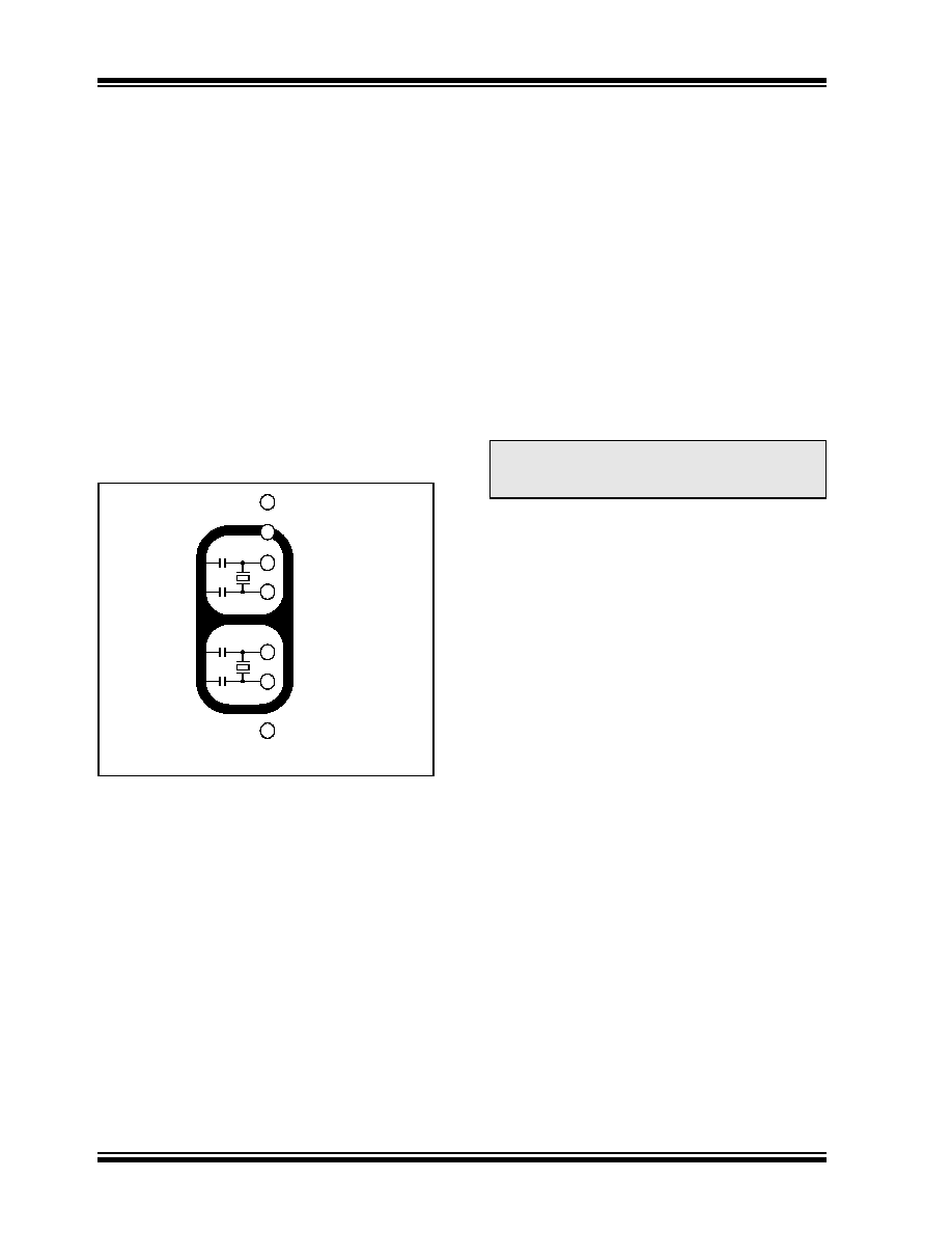
The oscillator circuit, shown in Figure 13-3, should be
located as close as possible to the microcontroller.
There should be no circuits passing within the oscillator
circuit boundaries other than VSS or VDD.
If a high-speed circuit must be located near the oscilla-
tor (such as the CCP1 pin in Output Compare or PWM
mode, or the primary oscillator using the OSC2 pin), a
grounded guard ring around the oscillator circuit, as
shown in Figure 13-4, may be helpful when used on a
single-sided PCB or in addition to a ground plane.
FIGURE 13-4:
OSCILLATOR CIRCUIT
WITH GROUNDED
GUARD RING
13.4
Timer1 Interrupt
The TMR1 register pair (TMR1H:TMR1L) increments
from 0000h to FFFFh and rolls over to 0000h. The
Timer1 interrupt, if enabled, is generated on overflow
which is latched in interrupt flag bit, TMR1IF
(PIR1<0>). This interrupt can be enabled or disabled
by setting or clearing the Timer1 Interrupt Enable bit,
TMR1IE (PIE1<0>).
13.5
Resetting Timer1 Using the CCPx
Special Event Trigger
If CCP1 or CCP2 is configured to use Timer1 and to
generate a Special Event Trigger in Compare mode
(CCPxM<3:0> = 1011), this signal will reset Timer3.
The trigger from CCP2 will also start an A/D conversion
if the A/D module is enabled (see Section 16.3.4
“Special Event Trigger” for more information).
The module must be configured as either a timer or a
synchronous counter to take advantage of this feature.
When used this way, the CCPRxH:CCPRxL register
pair effectively becomes a Period register for Timer1.
If Timer1 is running in Asynchronous Counter mode,
this Reset operation may not work.
In the event that a write to Timer1 coincides with a
Special Event Trigger, the write operation will take
precedence.
13.6
Using Timer1 as a Real-Time Clock
Adding an external LP oscillator to Timer1 (such as the
one described in Section 13.3 “Timer1 Oscillator”
above) gives users the option to include RTC function-
ality to their applications. This is accomplished with an
inexpensive watch crystal to provide an accurate time
base and several lines of application code to calculate
the time. When operating in Sleep mode and using a
battery or supercapacitor as a power source, it can
completely eliminate the need for a separate RTC
device and battery backup.
The application code routine, RTCisr, shown in
Example 13-1, demonstrates a simple method to
increment a counter at one-second intervals using an
Interrupt Service Routine. Incrementing the TMR1
register pair to overflow triggers the interrupt and calls
the routine which increments the seconds counter by
one. Additional counters for minutes and hours are
incremented as the previous counter overflows.
Since the register pair is 16 bits wide, counting up to
overflow the register directly from a 32.768 kHz clock
would take 2 seconds. To force the overflow at the
required one-second intervals, it is necessary to pre-
load it. The simplest method is to set the MSb of
TMR1H with a BSF instruction. Note that the TMR1L
register is never preloaded or altered; doing so may
introduce cumulative error over many cycles.
For this method to be accurate, Timer1 must operate in
Asynchronous mode and the Timer1 overflow interrupt
must be enabled (PIE1<0> = 1), as shown in the
routine, RTCinit. The Timer1 oscillator must also be
enabled and running at all times.
VDD
OSC1
VSS
OSC2
RC0
RC1
RC2
Note: Not drawn to scale.
Note:
The Special Event Triggers from the CCPx
module will not set the TMR1IF interrupt
flag bit (PIR1<0>).
相关PDF资料 |
PDF描述 |
|---|---|
| VE-J1Z-IW-B1 | CONVERTER MOD DC/DC 2V 40W |
| MC74HC4052ADTR2G | IC MUX/DEMUX DUAL 4X1 16TSSOP |
| VE-J1Y-IX-B1 | CONVERTER MOD DC/DC 3.3V 49.5W |
| VI-J1Z-IX-B1 | CONVERTER MOD DC/DC 2V 30W |
| PIC18F67J93-I/PT | IC PIC MCU FLASH 128KX4 64-TQFP |
相关代理商/技术参数 |
参数描述 |
|---|---|
| PIC18F46K20-E/ML | 功能描述:8位微控制器 -MCU 64KB Flash 3968B RAM 36 I/O 8B RoHS:否 制造商:Silicon Labs 核心:8051 处理器系列:C8051F39x 数据总线宽度:8 bit 最大时钟频率:50 MHz 程序存储器大小:16 KB 数据 RAM 大小:1 KB 片上 ADC:Yes 工作电源电压:1.8 V to 3.6 V 工作温度范围:- 40 C to + 105 C 封装 / 箱体:QFN-20 安装风格:SMD/SMT |
| PIC18F46K20-E/MV | 功能描述:8位微控制器 -MCU 64KB FL 3968b RAM 8b Familynanowatt XLP RoHS:否 制造商:Silicon Labs 核心:8051 处理器系列:C8051F39x 数据总线宽度:8 bit 最大时钟频率:50 MHz 程序存储器大小:16 KB 数据 RAM 大小:1 KB 片上 ADC:Yes 工作电源电压:1.8 V to 3.6 V 工作温度范围:- 40 C to + 105 C 封装 / 箱体:QFN-20 安装风格:SMD/SMT |
| PIC18F46K20-E/P | 功能描述:8位微控制器 -MCU 64KB Flash 3968B RAM 36 I/O 8B RoHS:否 制造商:Silicon Labs 核心:8051 处理器系列:C8051F39x 数据总线宽度:8 bit 最大时钟频率:50 MHz 程序存储器大小:16 KB 数据 RAM 大小:1 KB 片上 ADC:Yes 工作电源电压:1.8 V to 3.6 V 工作温度范围:- 40 C to + 105 C 封装 / 箱体:QFN-20 安装风格:SMD/SMT |
| PIC18F46K20-E/PT | 功能描述:8位微控制器 -MCU 64KB Flash 3968B RAM 36 I/O 8B RoHS:否 制造商:Silicon Labs 核心:8051 处理器系列:C8051F39x 数据总线宽度:8 bit 最大时钟频率:50 MHz 程序存储器大小:16 KB 数据 RAM 大小:1 KB 片上 ADC:Yes 工作电源电压:1.8 V to 3.6 V 工作温度范围:- 40 C to + 105 C 封装 / 箱体:QFN-20 安装风格:SMD/SMT |
| PIC18F46K20-I/ML | 功能描述:8位微控制器 -MCU 64KB Flash 3968B RAM 36 I/O 8B RoHS:否 制造商:Silicon Labs 核心:8051 处理器系列:C8051F39x 数据总线宽度:8 bit 最大时钟频率:50 MHz 程序存储器大小:16 KB 数据 RAM 大小:1 KB 片上 ADC:Yes 工作电源电压:1.8 V to 3.6 V 工作温度范围:- 40 C to + 105 C 封装 / 箱体:QFN-20 安装风格:SMD/SMT |
发布紧急采购,3分钟左右您将得到回复。