参数资料
| 型号: | PIC18LF4331T-I/ML |
| 厂商: | Microchip Technology |
| 文件页数: | 51/119页 |
| 文件大小: | 0K |
| 描述: | IC MCU FLASH 4KX16 44QFN |
| 标准包装: | 1,600 |
| 系列: | PIC® 18F |
| 核心处理器: | PIC |
| 芯体尺寸: | 8-位 |
| 速度: | 40MHz |
| 连通性: | I²C,SPI,UART/USART |
| 外围设备: | 欠压检测/复位,LVD,电源控制 PWM,QEI,POR,PWM,WDT |
| 输入/输出数: | 36 |
| 程序存储器容量: | 8KB(4K x 16) |
| 程序存储器类型: | 闪存 |
| EEPROM 大小: | 256 x 8 |
| RAM 容量: | 768 x 8 |
| 电压 - 电源 (Vcc/Vdd): | 2 V ~ 5.5 V |
| 数据转换器: | A/D 9x10b |
| 振荡器型: | 内部 |
| 工作温度: | -40°C ~ 85°C |
| 封装/外壳: | 44-VQFN 裸露焊盘 |
| 包装: | 带卷 (TR) |
第1页第2页第3页第4页第5页第6页第7页第8页第9页第10页第11页第12页第13页第14页第15页第16页第17页第18页第19页第20页第21页第22页第23页第24页第25页第26页第27页第28页第29页第30页第31页第32页第33页第34页第35页第36页第37页第38页第39页第40页第41页第42页第43页第44页第45页第46页第47页第48页第49页第50页当前第51页第52页第53页第54页第55页第56页第57页第58页第59页第60页第61页第62页第63页第64页第65页第66页第67页第68页第69页第70页第71页第72页第73页第74页第75页第76页第77页第78页第79页第80页第81页第82页第83页第84页第85页第86页第87页第88页第89页第90页第91页第92页第93页第94页第95页第96页第97页第98页第99页第100页第101页第102页第103页第104页第105页第106页第107页第108页第109页第110页第111页第112页第113页第114页第115页第116页第117页第118页第119页
2010 Microchip Technology Inc.
DS39616D-page 37
PIC18F2331/2431/4331/4431
3.7.2
OSCILLATOR TRANSITIONS
The PIC18F2331/2431/4331/4431 devices contain
circuitry to prevent clocking “glitches” when switching
between clock sources. A short pause in the system
clock occurs during the clock switch. The length of this
pause is between 8 and 9 clock periods of the new
clock source. This ensures that the new clock source is
stable and that its pulse width will not be less than the
shortest pulse width of the two clock sources.
Clock transitions are discussed in greater detail in
.
3.8
Effects of Power-Managed Modes
on the Various Clock Sources
When PRI_IDLE mode is selected, the designated
primary oscillator continues to run without interruption.
For all other power-managed modes, the oscillator using
the OSC1 pin is disabled. The OSC1 pin (and OSC2 pin,
if used by the oscillator) will stop oscillating.
When the device executes a SLEEP instruction, the
system is switched to one of the power-managed
modes, depending on the state of the IDLEN and
SCS<1:0> bits of the OSCCON register. See
for details.
In
secondary
clock
modes
(SEC_RUN
and
SEC_IDLE), the Timer1 oscillator is operating and
providing the system clock. The Timer1 oscillator may
also run in all power-managed modes if required to
clock Timer1.
In internal oscillator modes (RC_RUN and RC_IDLE),
the internal oscillator block provides the system clock
source. The INTRC output can be used directly to
provide the system clock and may be enabled to
support various special features, regardless of the
power-managed mode (see Section 23.2 “Watchdog
through Section 23.4 “Fail-Safe Clock
). The INTOSC output at 8 MHz may be used
directly to clock the system, or may be divided down
first. The INTOSC output is disabled if the system clock
is provided directly from the INTRC output.
If the Sleep mode is selected, all clock sources are
stopped. Since all the transistor switching currents
have been stopped, Sleep mode achieves the lowest
current consumption of the device (only leakage
currents).
Enabling any on-chip feature that will operate during
Sleep will increase the current consumed during Sleep.
The INTRC is required to support WDT operation. The
Timer1 oscillator may be operating to support a Real-
Time Clock. Other features may be operating that do
not require a system clock source (i.e., SSP slave,
INTx pins, A/D conversions and others).
3.9
Power-up Delays
Power-up delays are controlled by two timers, so that no
external Reset circuitry is required for most applications.
The delays ensure that the device is kept in Reset until
the device power supply is stable under normal
circumstances, and the primary clock is operating and
stable. For additional information on power-up delays,
see Section 5.3 “Power-on Reset (POR)” through
The first timer is the Power-up Timer (PWRT), which
provides a fixed delay on power-up (parameter 33,
Table 26-8), if enabled, in Configuration Register 2L.
The second timer is the Oscillator Start-up Timer
(OST), intended to keep the chip in Reset until the crys-
tal oscillator is stable (LP, XT and HS modes). The OST
does this by counting 1024 oscillator cycles before
allowing the oscillator to clock the device.
When the HSPLL Oscillator mode is selected, the
device is kept in Reset for an additional 2 ms, following
the HS mode OST delay, so the PLL can lock to the
incoming clock frequency.
TABLE 3-3:
OSC1 AND OSC2 PIN STATES IN SLEEP MODE
OSC Mode
OSC1 Pin
OSC2 Pin
RC, INTIO1
Floating, external resistor
should pull high
At logic low (clock/4 output)
RCIO, INTIO2
Floating, external resistor
should pull high
Configured as PORTA, bit 6
ECIO
Floating, pulled by external clock
Configured as PORTA, bit 6
EC
Floating, pulled by external clock
At logic low (clock/4 output)
LP, XT and HS
Feedback inverter disabled at
quiescent voltage level
Feedback inverter disabled at
quiescent voltage level
Note:
See Table 5-1 in Section 5.0 “Reset” for time-outs due to Sleep and MCLR Reset.
相关PDF资料 |
PDF描述 |
|---|---|
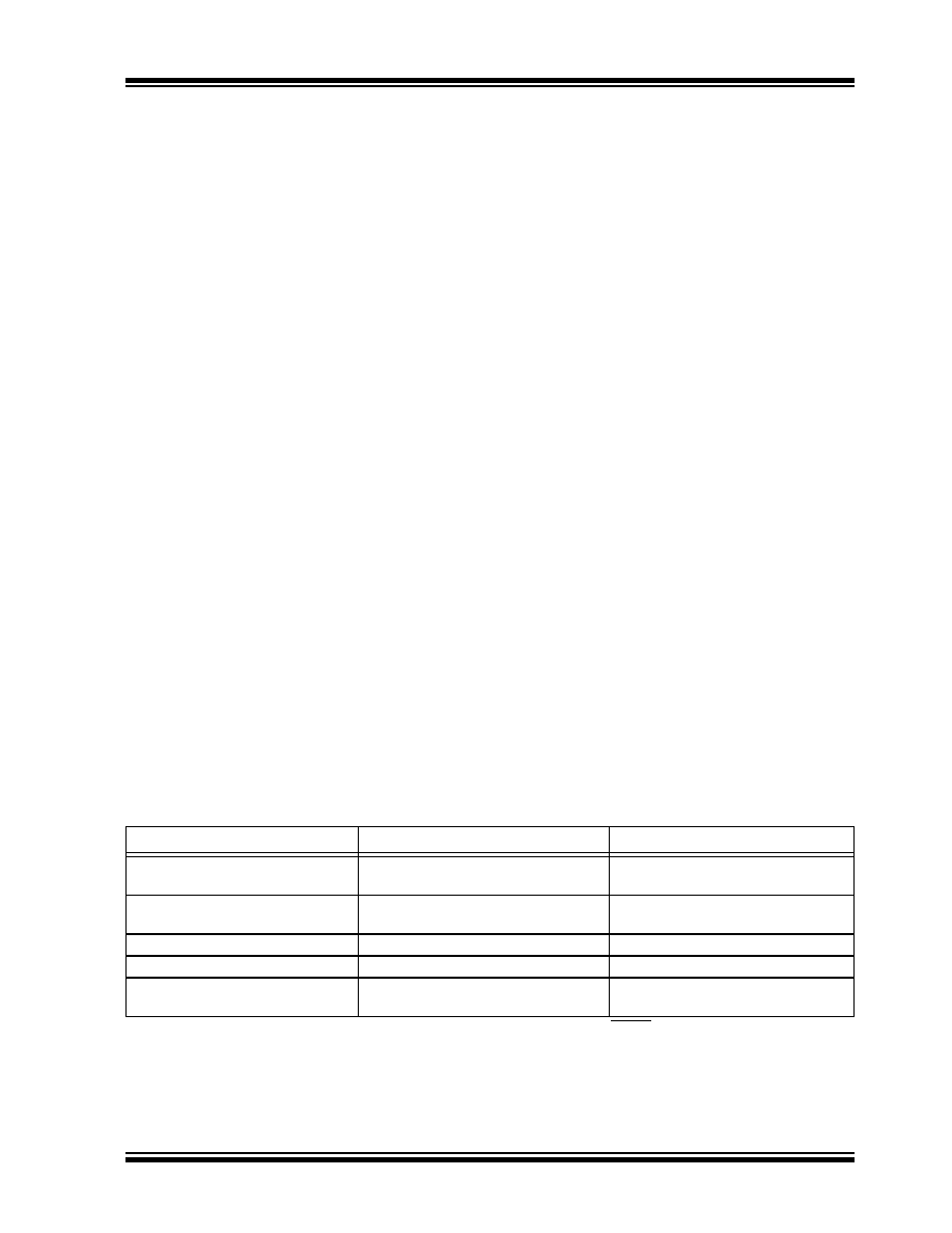
| PIC16C56A-04I/SO | IC MCU OTP 1KX12 18SOIC |
| PIC18F4515T-I/ML | IC MCU FLASH 24KX16 44QFN |
| PIC18F4515-E/PT | IC MCU FLASH 24KX16 44TQFP |
| PIC18F4515-E/ML | IC MCU FLASH 24KX16 44QFN |
| PIC18LF2610T-I/SO | IC MCU FLASH 32KX16 28SOIC |
相关代理商/技术参数 |
参数描述 |
|---|---|
| PIC18LF43K22-E/ML | 功能描述:8位微控制器 -MCU 8KB Flash 3968b RAM SERIAL EE IND RoHS:否 制造商:Silicon Labs 核心:8051 处理器系列:C8051F39x 数据总线宽度:8 bit 最大时钟频率:50 MHz 程序存储器大小:16 KB 数据 RAM 大小:1 KB 片上 ADC:Yes 工作电源电压:1.8 V to 3.6 V 工作温度范围:- 40 C to + 105 C 封装 / 箱体:QFN-20 安装风格:SMD/SMT |
| PIC18LF43K22-E/MV | 功能描述:8位微控制器 -MCU 8KB FL 512b RAM 8bit familynanoWatt XLP RoHS:否 制造商:Silicon Labs 核心:8051 处理器系列:C8051F39x 数据总线宽度:8 bit 最大时钟频率:50 MHz 程序存储器大小:16 KB 数据 RAM 大小:1 KB 片上 ADC:Yes 工作电源电压:1.8 V to 3.6 V 工作温度范围:- 40 C to + 105 C 封装 / 箱体:QFN-20 安装风格:SMD/SMT |
| PIC18LF43K22-E/P | 功能描述:8位微控制器 -MCU 8KB Flash 3968b RAM SERIAL EE IND RoHS:否 制造商:Silicon Labs 核心:8051 处理器系列:C8051F39x 数据总线宽度:8 bit 最大时钟频率:50 MHz 程序存储器大小:16 KB 数据 RAM 大小:1 KB 片上 ADC:Yes 工作电源电压:1.8 V to 3.6 V 工作温度范围:- 40 C to + 105 C 封装 / 箱体:QFN-20 安装风格:SMD/SMT |
| PIC18LF43K22-E/PT | 功能描述:8位微控制器 -MCU 8KB Flash 3968b RAM SERIAL EE IND RoHS:否 制造商:Silicon Labs 核心:8051 处理器系列:C8051F39x 数据总线宽度:8 bit 最大时钟频率:50 MHz 程序存储器大小:16 KB 数据 RAM 大小:1 KB 片上 ADC:Yes 工作电源电压:1.8 V to 3.6 V 工作温度范围:- 40 C to + 105 C 封装 / 箱体:QFN-20 安装风格:SMD/SMT |
| PIC18LF43K22-I/ML | 功能描述:8位微控制器 -MCU 8KB Flash 3968b RAM SERIAL EE IND RoHS:否 制造商:Silicon Labs 核心:8051 处理器系列:C8051F39x 数据总线宽度:8 bit 最大时钟频率:50 MHz 程序存储器大小:16 KB 数据 RAM 大小:1 KB 片上 ADC:Yes 工作电源电压:1.8 V to 3.6 V 工作温度范围:- 40 C to + 105 C 封装 / 箱体:QFN-20 安装风格:SMD/SMT |
发布紧急采购,3分钟左右您将得到回复。