参数资料
| 型号: | PPC5606BCLU64 |
| 厂商: | Freescale Semiconductor |
| 文件页数: | 45/112页 |
| 文件大小: | 0K |
| 描述: | MCU 32BIT 1M 64MHZ |
| 标准包装: | 40 |
| 系列: | MPC56xx Qorivva |
| 核心处理器: | e200z0h |
| 芯体尺寸: | 32-位 |
| 速度: | 64MHz |
| 连通性: | CAN,I²C,LIN,SCI,SPI |
| 外围设备: | POR,PWM,WDT |
| 输入/输出数: | 149 |
| 程序存储器容量: | 1MB(1M x 8) |
| 程序存储器类型: | 闪存 |
| EEPROM 大小: | 4K x 16 |
| RAM 容量: | 80K x 8 |
| 电压 - 电源 (Vcc/Vdd): | 3 V ~ 3.6 V |
| 数据转换器: | A/D 29x10b,5x12b |
| 振荡器型: | 内部 |
| 工作温度: | -40°C ~ 85°C |
| 封装/外壳: | 176-LQFP |
| 包装: | 托盘 |
第1页第2页第3页第4页第5页第6页第7页第8页第9页第10页第11页第12页第13页第14页第15页第16页第17页第18页第19页第20页第21页第22页第23页第24页第25页第26页第27页第28页第29页第30页第31页第32页第33页第34页第35页第36页第37页第38页第39页第40页第41页第42页第43页第44页当前第45页第46页第47页第48页第49页第50页第51页第52页第53页第54页第55页第56页第57页第58页第59页第60页第61页第62页第63页第64页第65页第66页第67页第68页第69页第70页第71页第72页第73页第74页第75页第76页第77页第78页第79页第80页第81页第82页第83页第84页第85页第86页第87页第88页第89页第90页第91页第92页第93页第94页第95页第96页第97页第98页第99页第100页第101页第102页第103页第104页第105页第106页第107页第108页第109页第110页第111页第112页
MPC5607B Microcontroller Data Sheet, Rev. 7
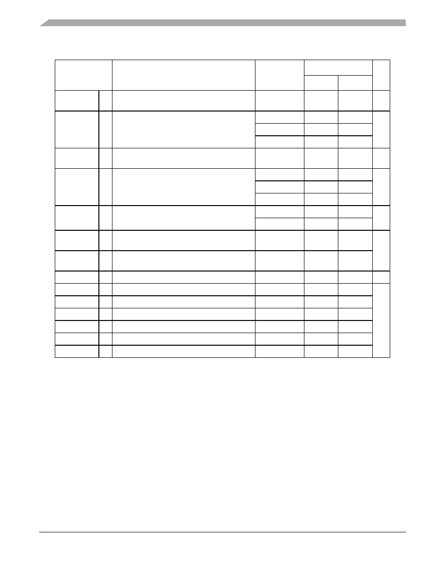
Electrical characteristics
Freescale Semiconductor
38
NOTE
RAM data retention is guaranteed with VDD_LV not below 1.08 V.
VSS_LV
3
SR Voltage on VSS_LV (low voltage digital supply)
pins with respect to ground (VSS)
—VSS 0.1 VSS +0.1
V
VDD_BV
4
SR Voltage on VDD_BV pin (regulator supply) with
respect to ground (VSS)
—4.5
5.5
V
Voltage drop2
3.0
5.5
Relative to VDD
3.0
VDD +0.1
VSS_ADC
SR Voltage on VSS_HV_ADC0, VSS_HV_ADC1
(ADC reference) pin with respect to ground (VSS)
—VSS 0.1 VSS +0.1
V
VDD_ADC
5
SR Voltage on VDD_HV_ADC0, VDD_HV_ADC1
(ADC reference) with respect to ground (VSS)
—4.5
5.5
V
Voltage drop2
3.0
5.5
Relative to VDD VDD 0.1 VDD +0.1
VIN
SR Voltage on any GPIO pin with respect to ground
(VSS)
—VSS 0.1
—
V
Relative to VDD
—VDD +0.1
IINJPAD
SR Injected input current on any pin during overload
condition
—
55
mA
IINJSUM
SR Absolute sum of all injected input currents during
overload condition
—
50
TVDD
SR VDD slope to ensure correct power up
6
—
0.25
V/s
TA C-Grade Part SR Ambient temperature under bias
fCPU 64 MHz
7
40
85
°C
TJ C-Grade Part SR Junction temperature under bias
—
40
110
TA V-Grade Part SR Ambient temperature under bias
fCPU 64 MHz
40
105
TJ V-Grade Part SR Junction temperature under bias
—
40
130
TA M-Grade Part SR Ambient temperature under bias
fCPU 64 MHz
40
125
TJ M-Grade Part SR Junction temperature under bias
—
40
150
1 100 nF capacitance needs to be provided between each V
DD/VSS pair.
2 Full device operation is guaranteed by design when the voltage drops below 4.5 V down to 3.0 V. However, certain
analog electrical characteristics will not be guaranteed to stay within the stated limits.
3 330 nF capacitance needs to be provided between each V
DD_LV/VSS_LV supply pair.
4 470 nF capacitance needs to be provided between V
DD_BV and the nearest VSS_LV (higher value may be needed
depending on external regulator characteristics). While the supply voltage ramps up, the slope on VDD_BV should
be less than 0.9VDD_HV in order to ensure the device does not enter regulator bypass mode.
5 100 nF capacitance needs to be provided between V
DD_ADC/VSS_ADC pair.
6 Guaranteed by device validation
7 When the FMPLL uses the frequency modulation with a modulation depth of 4% from the center spread frequency,
the maximum value of fCPU is 66.56 MHz.
Table 13. Recommended operating conditions (5.0 V) (continued)
Symbol
Parameter
Conditions
Value
Unit
Min
Max
相关PDF资料 |
PDF描述 |
|---|---|
| PPC8309VMAGDCA | MPU POWERQUICC II PRO 489-MAP |
| PS302CSA | IC SWITCH SPST 8SOIC |
| PS321CPA | IC SWITCH DUAL SPST 8DIP |
| PS323CUAEX | IC ANLG SW SPST DUAL NO 8-MSOP |
| PS383CSE | IC SWITCH DUAL SPDT 16SOIC |
相关代理商/技术参数 |
参数描述 |
|---|---|
| PPC5606BECLLR | 制造商:FREESCALE 制造商全称:Freescale Semiconductor, Inc 功能描述:Microcontroller |
| PPC5606BECLQ | 制造商:FREESCALE 制造商全称:Freescale Semiconductor, Inc 功能描述:Microcontroller |
| PPC5606BECLQR | 制造商:FREESCALE 制造商全称:Freescale Semiconductor, Inc 功能描述:Microcontroller |
| PPC5606BECLU | 制造商:FREESCALE 制造商全称:Freescale Semiconductor, Inc 功能描述:Microcontroller |
| PPC5606BECLUR | 制造商:FREESCALE 制造商全称:Freescale Semiconductor, Inc 功能描述:Microcontroller |
发布紧急采购,3分钟左右您将得到回复。