- 您现在的位置:买卖IC网 > PDF目录368232 > PSD813FH Field Programmble Microcontroller Peripherals With Flash Memory(带闪存的现场可编程微控制器) PDF资料下载
参数资料
| 型号: | PSD813FH |
| 英文描述: | Field Programmble Microcontroller Peripherals With Flash Memory(带闪存的现场可编程微控制器) |
| 中文描述: | 场可编程微控制器外围设备与快闪记忆体(带闪存的现场可编程微控制器) |
| 文件页数: | 7/83页 |
| 文件大小: | 369K |
| 代理商: | PSD813FH |
第1页第2页第3页第4页第5页第6页当前第7页第8页第9页第10页第11页第12页第13页第14页第15页第16页第17页第18页第19页第20页第21页第22页第23页第24页第25页第26页第27页第28页第29页第30页第31页第32页第33页第34页第35页第36页第37页第38页第39页第40页第41页第42页第43页第44页第45页第46页第47页第48页第49页第50页第51页第52页第53页第54页第55页第56页第57页第58页第59页第60页第61页第62页第63页第64页第65页第66页第67页第68页第69页第70页第71页第72页第73页第74页第75页第76页第77页第78页第79页第80页第81页第82页第83页
Prelimnary
PSD813FN/FH
7
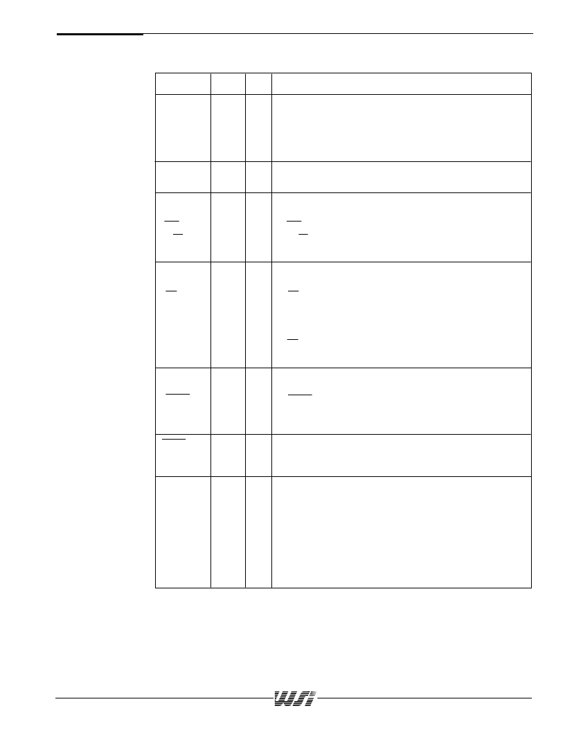
The following table describes the pin names and pin functions of the PSD813FN/FH. Pins
that have multiple names and/or functions are defined by configuration.
Table 3.
PSD813FN/FH
Pin
Descriptions
Pin Name
Pin
Type
Function Description
ADIO0–7
30–37
I/O
Address/Data Port, interface to Microcontroller Bus
1. Input pins for multiplexed low order address/data byte.
ALE or AS latches address A0-7 for input to PLDs.
The PSD drives data out only if read is active and one of
the internal PSD functional blocks is selected.
A8–15
39–46
I/O
Address Port, interface to Microcontroller Bus
1. Address A8-15 inputs.
CNTL0
47
I
Write Input pin with multiple configurations. Depending on
the MCU interface selected, this pin can be:
1. WR – active low write input
2. R_W – read/write pin, low for write bus cycle
3. Control signal (CNTL0) input to PLD
(WR,
R_W)
CNTL1
50
I
Read or Data Strobe Input pin with multiple configurations.
Depending on the MCU interface selected, this pin can be:
1. RD – active low read input
2. E – E clock input.
During a write bus cycle, E is high and R/W is low
During a read bus cycle, E is high and R/W is high
3. DS – Data Strobe, active low
4. Control signal (CNTL1) input to PLD
(RD,
E, DS)
CNTL2
49
I
Read or other Control input pin with multiple configurations.
Depending on the MCU interface selected, this pin can be:
1. PSEN – Program Select enable, active low in code fetch
bus cycle
2. Control signal (CNTL2) input or general input to PLD
(PSEN)
Reset
48
I
Active low input. Resets I/O Ports, PLD Micro
Cells and
some of the Configuration Registers. Must be active at
power up.
PA0
PA1
PA2
PA3
29
28
27
25
I/O
Port A, PA0 – 3. This port is pin configurable and has
multiple functions:
1. MCU I/O – standard output or input port
2. External chip select (ECSPLD) output, or input to GPLD
3. Latched address outputs (see Table 4)
4. As Data Bus Port (D0–3) in non-multiplexed bus
configuration
5. Peripheral I/O mode
相关PDF资料 |
PDF描述 |
|---|---|
| PSD82 | Three Phase Rectifier Bridges |
| PSD834F2V | Flash PSD, 3.3V Supply, for 8-bit MCUs 2 Mbit + 256 Kbit Dual Flash Memories and 64 Kbit SRAM(2M位+256K位双路闪速存储器和64K位静态RAM,闪速PSD,3.3V电源,用于8位MCU.) |
| PSD834F2 | Flash In-System Programmable (ISP) Peripherals For 8-bit MCUs(用于8位MCUs的闪速ISP外围) |
| PSD835G2 | Configurable Memory System on a Chip for 8-Bit Microcontrollers(8位微控制器片上存储器可编程外设) |
| PSD835G2 | 100V 100kRad Hi-Rel Single N-Channel TID Hardened MOSFET in a TO-254AA Tabless package; Similar to IRHMJ57160 with optional Total Dose Rating of 1000kRads |
相关代理商/技术参数 |
参数描述 |
|---|---|
| PSD813FH-15J | 制造商:WSI 功能描述: |
| PSD813FH-90J | 制造商:WSI 功能描述: |
| PSD813FN-15J | 制造商:WSI 功能描述: |
| PSD833F2-90J | 功能描述:CPLD - 复杂可编程逻辑器件 5.0V 1M 90ns RoHS:否 制造商:Lattice 系列: 存储类型:EEPROM 大电池数量:128 最大工作频率:333 MHz 延迟时间:2.7 ns 可编程输入/输出端数量:64 工作电源电压:3.3 V 最大工作温度:+ 90 C 最小工作温度:0 C 封装 / 箱体:TQFP-100 |
| PSD833F2-90JI | 功能描述:SPLD - 简单可编程逻辑器件 5.0V 1M 90ns RoHS:否 制造商:Texas Instruments 逻辑系列:TICPAL22V10Z 大电池数量:10 最大工作频率:66 MHz 延迟时间:25 ns 工作电源电压:4.75 V to 5.25 V 电源电流:100 uA 最大工作温度:+ 75 C 最小工作温度:0 C 安装风格:Through Hole 封装 / 箱体:DIP-24 |
发布紧急采购,3分钟左右您将得到回复。