- 您现在的位置:买卖IC网 > PDF目录69310 > R5F213J5TNNP MICROCONTROLLER, QCC40 PDF资料下载
参数资料
| 型号: | R5F213J5TNNP |
| 元件分类: | 微控制器/微处理器 |
| 英文描述: | MICROCONTROLLER, QCC40 |
| 封装: | 5 X 5 MM, 0.40 MM PITCH, QFN-40 |
| 文件页数: | 10/45页 |
| 文件大小: | 440K |
| 代理商: | R5F213J5TNNP |
第1页第2页第3页第4页第5页第6页第7页第8页第9页当前第10页第11页第12页第13页第14页第15页第16页第17页第18页第19页第20页第21页第22页第23页第24页第25页第26页第27页第28页第29页第30页第31页第32页第33页第34页第35页第36页第37页第38页第39页第40页第41页第42页第43页第44页第45页
18
ATtiny4/5/9/10 [DATASHEET]
8127F–AVR–02/2013
6.1.4
ADC Clock – clk
ADC
The ADC is provided with a dedicated clock domain. This allows halting the CPU and I/O clocks in order to reduce
noise generated by digital circuitry. This gives more accurate ADC conversion results.
The ADC is available in ATtiny5/10, only.
6.2
Clock Sources
All synchronous clock signals are derived from the main clock. The device has three alternative sources for the
main clock, as follows:
External Clock (see page 18)
See Table 6-3 on page 21 on how to select and change the active clock source.
6.2.1
Calibrated Internal 8 MHz Oscillator
The calibrated internal oscillator provides an approximately 8 MHz clock signal. Though voltage and temperature
dependent, this clock can be very accurately calibrated by the user. See Table 16-2 on page 117, Figure 17-39 on
page 141 and Figure 17-40 on page 141 for more details.
This clock may be selected as the main clock by setting the Clock Main Select bits CLKMS[1:0] in CLKMSR to
0b00. Once enabled, the oscillator will operate with no external components. During reset, hardware loads the cal-
ibration byte into the OSCCAL register and thereby automatically calibrates the oscillator. The accuracy of this
calibration is shown as Factory calibration in Table 16-2 on page 117.
When this oscillator is used as the main clock, the watchdog oscillator will still be used for the watchdog timer and
reset time-out. For more information on the pre-programmed calibration value, see section “Calibration Section” on
6.2.2
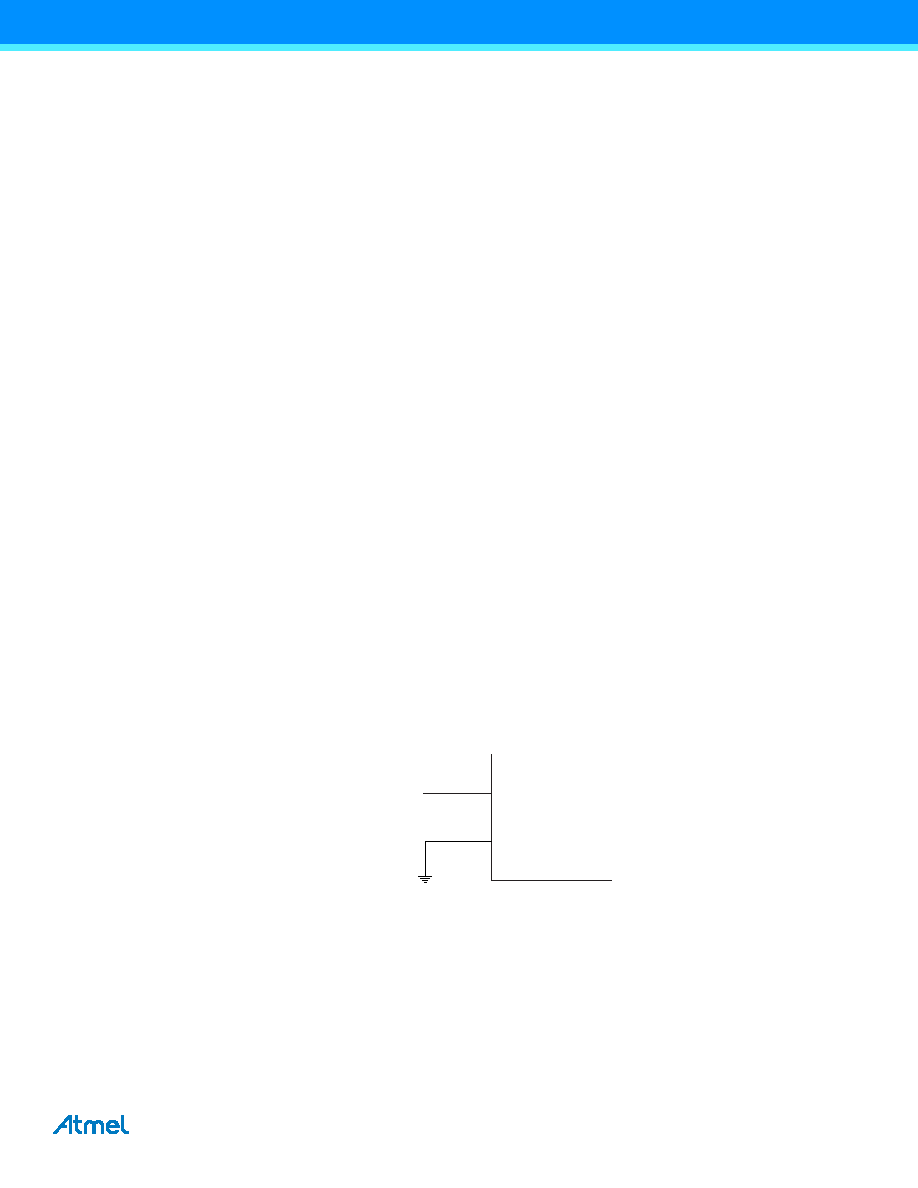
External Clock
To use the device with an external clock source, CLKI should be driven as shown in Figure 6-2. The external clock
is selected as the main clock by setting CLKMS[1:0] bits in CLKMSR to 0b10.
Figure 6-2.
External Clock Drive Configuration
When applying an external clock, it is required to avoid sudden changes in the applied clock frequency to ensure
stable operation of the MCU. A variation in frequency of more than 2% from one clock cycle to the next can lead to
unpredictable behavior. It is required to ensure that the MCU is kept in reset during such changes in the clock
frequency.
EXTERNAL
CLOCK
SIGNAL
CLKI
GND
相关PDF资料 |
PDF描述 |
|---|---|
| R5F2L35ACDFP | 8-BIT, FLASH, 20 MHz, MICROCONTROLLER, PQFP52 |
| R5F2L368ANFA | 8-BIT, FLASH, 20 MHz, MICROCONTROLLER, PQFP64 |
| R5F2L3ACADFA | 8-BIT, FLASH, 20 MHz, MICROCONTROLLER, PQFP100 |
| R5F2L388ANFP | 8-BIT, FLASH, 20 MHz, MICROCONTROLLER, PQFP80 |
| R5F2L388ADFA | 8-BIT, FLASH, 20 MHz, MICROCONTROLLER, PQFP80 |
相关代理商/技术参数 |
参数描述 |
|---|---|
| R5F213J5TNNP#W4 | 功能描述:MCU 24KB ROM 2KB RAM 40-QFN RoHS:是 类别:集成电路 (IC) >> 嵌入式 - 微控制器, 系列:R8C/3x/3JT 标准包装:250 系列:80C 核心处理器:8051 芯体尺寸:8-位 速度:16MHz 连通性:EBI/EMI,I²C,UART/USART 外围设备:POR,PWM,WDT 输入/输出数:40 程序存储器容量:- 程序存储器类型:ROMless EEPROM 大小:- RAM 容量:256 x 8 电压 - 电源 (Vcc/Vdd):4.5 V ~ 5.5 V 数据转换器:A/D 8x10b 振荡器型:内部 工作温度:-40°C ~ 85°C 封装/外壳:68-LCC(J 形引线) 包装:带卷 (TR) |
| R5F213J6ANNP | 制造商:RENESAS 制造商全称:Renesas Technology Corp 功能描述:RENESAS MCU |
| R5F213J6CNNP | 制造商:RENESAS 制造商全称:Renesas Technology Corp 功能描述:RENESAS MCU |
| R5F213J6CNNP#U0 | 功能描述:MCU 1KB FLASH 32K ROM 36-QFN RoHS:是 类别:集成电路 (IC) >> 嵌入式 - 微控制器, 系列:R8C/3x/3JC 标准包装:250 系列:LPC11Uxx 核心处理器:ARM? Cortex?-M0 芯体尺寸:32-位 速度:50MHz 连通性:I²C,Microwire,SPI,SSI,SSP,UART/USART,USB 外围设备:欠压检测/复位,POR,WDT 输入/输出数:40 程序存储器容量:96KB(96K x 8) 程序存储器类型:闪存 EEPROM 大小:4K x 8 RAM 容量:10K x 8 电压 - 电源 (Vcc/Vdd):1.8 V ~ 3.6 V 数据转换器:A/D 8x10b 振荡器型:内部 工作温度:-40°C ~ 85°C 封装/外壳:48-LQFP 包装:托盘 其它名称:568-9587 |
| R5F213J6CNNP#W4 | 功能描述:MCU 32KB ROM 2.5KB RAM 36-QFN RoHS:是 类别:集成电路 (IC) >> 嵌入式 - 微控制器, 系列:R8C/3x/3JC 标准包装:300 系列:78K0R/Ix3 核心处理器:78K/0R 芯体尺寸:16-位 速度:40MHz 连通性:3 线 SIO,I²C,LIN,UART/USART 外围设备:DMA,LVD,POR,PWM,WDT 输入/输出数:27 程序存储器容量:16KB(16K x 8) 程序存储器类型:闪存 EEPROM 大小:- RAM 容量:1K x 8 电压 - 电源 (Vcc/Vdd):2.7 V ~ 5.5 V 数据转换器:A/D 8x10b 振荡器型:内部 工作温度:-40°C ~ 85°C 封装/外壳:38-SSOP 包装:托盘 |
发布紧急采购,3分钟左右您将得到回复。