- 您现在的位置:买卖IC网 > PDF目录69310 > R5F213J5TNNP MICROCONTROLLER, QCC40 PDF资料下载
参数资料
| 型号: | R5F213J5TNNP |
| 元件分类: | 微控制器/微处理器 |
| 英文描述: | MICROCONTROLLER, QCC40 |
| 封装: | 5 X 5 MM, 0.40 MM PITCH, QFN-40 |
| 文件页数: | 18/45页 |
| 文件大小: | 440K |
| 代理商: | R5F213J5TNNP |
第1页第2页第3页第4页第5页第6页第7页第8页第9页第10页第11页第12页第13页第14页第15页第16页第17页当前第18页第19页第20页第21页第22页第23页第24页第25页第26页第27页第28页第29页第30页第31页第32页第33页第34页第35页第36页第37页第38页第39页第40页第41页第42页第43页第44页第45页
25
ATtiny4/5/9/10 [DATASHEET]
8127F–AVR–02/2013
7.3.2
Analog to Digital Converter
If enabled, the ADC will be enabled in all sleep modes. To save power, the ADC should be disabled before entering
any sleep mode. When the ADC is turned off and on again, the next conversion will be an extended conversion.
See “Analog to Digital Converter” on page 82 for details on ADC operation.
The ADC is available in ATtiny5/10, only.
7.3.3
Watchdog Timer
If the Watchdog Timer is not needed in the application, this module should be turned off. If the Watchdog Timer is
enabled, it will be enabled in all sleep modes, and hence, always consume power. In the deeper sleep modes, this
will contribute significantly to the total current consumption. Refer to “Watchdog Timer” on page 30 for details on
how to configure the Watchdog Timer.
7.3.4
Port Pins
When entering a sleep mode, all port pins should be configured to use minimum power. The most important thing
is then to ensure that no pins drive resistive loads. In sleep modes where the I/O clock (clk
I/O) is stopped, the input
buffers of the device will be disabled. This ensures that no power is consumed by the input logic when not needed.
In some cases, the input logic is needed for detecting wake-up conditions, and it will then be enabled. Refer to the
section “Digital Input Enable and Sleep Modes” on page 44 for details on which pins are enabled. If the input buffer
is enabled and the input signal is left floating or has an analog signal level close to V
CC/2, the input buffer will use
excessive power.
For analog input pins, the digital input buffer should be disabled at all times. An analog signal level close to V
CC/2
on an input pin can cause significant current even in active mode. Digital input buffers can be disabled by writing to
the Digital Input Disable Register (DIDR0). Refer to “DIDR0 – Digital Input Disable Register 0” on page 81 for
details.
7.4
Register Description
7.4.1
SMCR – Sleep Mode Control Register
The SMCR Control Register contains control bits for power management.
Bits 7:4 – Res: Reserved Bits
These bits are reserved and will always read zero.
Bits 3:1 – SM2..SM0: Sleep Mode Select Bits 2..0
These bits select between available sleep modes, as shown in Table 7-2.
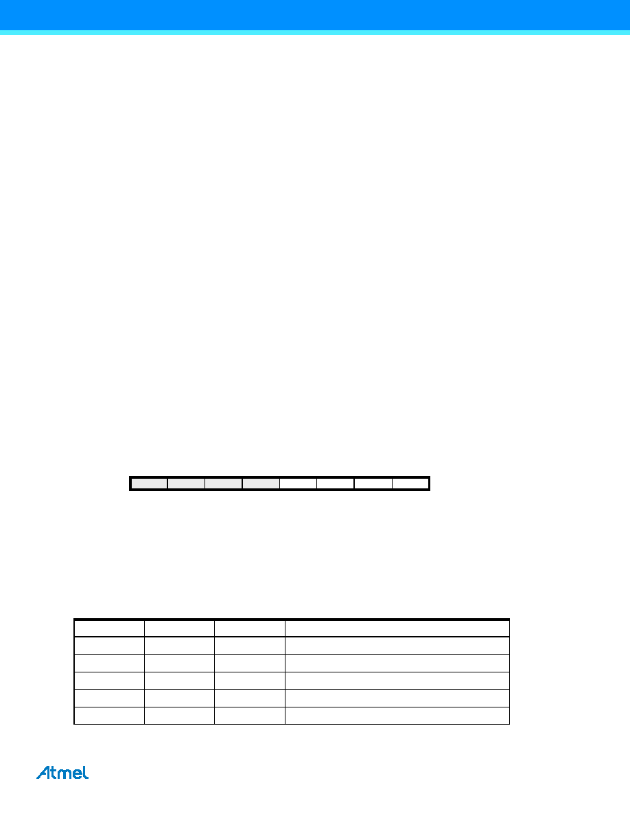
Bit
765
432
1
0
–
SM2
SM1
SM0
SE
SMCR
Read/Write
R
R/W
Initial Value
0
Table 7-2.
Sleep Mode Select
SM2
SM1
SM0
Sleep Mode
000
Idle
0
1
ADC noise reduction (1)
0
1
0
Power-down
011
Reserved
1
0
Standby
相关PDF资料 |
PDF描述 |
|---|---|
| R5F2L35ACDFP | 8-BIT, FLASH, 20 MHz, MICROCONTROLLER, PQFP52 |
| R5F2L368ANFA | 8-BIT, FLASH, 20 MHz, MICROCONTROLLER, PQFP64 |
| R5F2L3ACADFA | 8-BIT, FLASH, 20 MHz, MICROCONTROLLER, PQFP100 |
| R5F2L388ANFP | 8-BIT, FLASH, 20 MHz, MICROCONTROLLER, PQFP80 |
| R5F2L388ADFA | 8-BIT, FLASH, 20 MHz, MICROCONTROLLER, PQFP80 |
相关代理商/技术参数 |
参数描述 |
|---|---|
| R5F213J5TNNP#W4 | 功能描述:MCU 24KB ROM 2KB RAM 40-QFN RoHS:是 类别:集成电路 (IC) >> 嵌入式 - 微控制器, 系列:R8C/3x/3JT 标准包装:250 系列:80C 核心处理器:8051 芯体尺寸:8-位 速度:16MHz 连通性:EBI/EMI,I²C,UART/USART 外围设备:POR,PWM,WDT 输入/输出数:40 程序存储器容量:- 程序存储器类型:ROMless EEPROM 大小:- RAM 容量:256 x 8 电压 - 电源 (Vcc/Vdd):4.5 V ~ 5.5 V 数据转换器:A/D 8x10b 振荡器型:内部 工作温度:-40°C ~ 85°C 封装/外壳:68-LCC(J 形引线) 包装:带卷 (TR) |
| R5F213J6ANNP | 制造商:RENESAS 制造商全称:Renesas Technology Corp 功能描述:RENESAS MCU |
| R5F213J6CNNP | 制造商:RENESAS 制造商全称:Renesas Technology Corp 功能描述:RENESAS MCU |
| R5F213J6CNNP#U0 | 功能描述:MCU 1KB FLASH 32K ROM 36-QFN RoHS:是 类别:集成电路 (IC) >> 嵌入式 - 微控制器, 系列:R8C/3x/3JC 标准包装:250 系列:LPC11Uxx 核心处理器:ARM? Cortex?-M0 芯体尺寸:32-位 速度:50MHz 连通性:I²C,Microwire,SPI,SSI,SSP,UART/USART,USB 外围设备:欠压检测/复位,POR,WDT 输入/输出数:40 程序存储器容量:96KB(96K x 8) 程序存储器类型:闪存 EEPROM 大小:4K x 8 RAM 容量:10K x 8 电压 - 电源 (Vcc/Vdd):1.8 V ~ 3.6 V 数据转换器:A/D 8x10b 振荡器型:内部 工作温度:-40°C ~ 85°C 封装/外壳:48-LQFP 包装:托盘 其它名称:568-9587 |
| R5F213J6CNNP#W4 | 功能描述:MCU 32KB ROM 2.5KB RAM 36-QFN RoHS:是 类别:集成电路 (IC) >> 嵌入式 - 微控制器, 系列:R8C/3x/3JC 标准包装:300 系列:78K0R/Ix3 核心处理器:78K/0R 芯体尺寸:16-位 速度:40MHz 连通性:3 线 SIO,I²C,LIN,UART/USART 外围设备:DMA,LVD,POR,PWM,WDT 输入/输出数:27 程序存储器容量:16KB(16K x 8) 程序存储器类型:闪存 EEPROM 大小:- RAM 容量:1K x 8 电压 - 电源 (Vcc/Vdd):2.7 V ~ 5.5 V 数据转换器:A/D 8x10b 振荡器型:内部 工作温度:-40°C ~ 85°C 封装/外壳:38-SSOP 包装:托盘 |
发布紧急采购,3分钟左右您将得到回复。