- 您现在的位置:买卖IC网 > PDF目录69312 > R5F2L3AACDFP 8-BIT, FLASH, 20 MHz, MICROCONTROLLER, PQFP100 PDF资料下载
参数资料
| 型号: | R5F2L3AACDFP |
| 元件分类: | 微控制器/微处理器 |
| 英文描述: | 8-BIT, FLASH, 20 MHz, MICROCONTROLLER, PQFP100 |
| 封装: | 14 X 14 MM, 0.50 MM PITCH, PLASTIC, LQFP-100 |
| 文件页数: | 52/74页 |
| 文件大小: | 959K |
| 代理商: | R5F2L3AACDFP |
第1页第2页第3页第4页第5页第6页第7页第8页第9页第10页第11页第12页第13页第14页第15页第16页第17页第18页第19页第20页第21页第22页第23页第24页第25页第26页第27页第28页第29页第30页第31页第32页第33页第34页第35页第36页第37页第38页第39页第40页第41页第42页第43页第44页第45页第46页第47页第48页第49页第50页第51页当前第52页第53页第54页第55页第56页第57页第58页第59页第60页第61页第62页第63页第64页第65页第66页第67页第68页第69页第70页第71页第72页第73页第74页
57
2588F–AVR–06/2013
ATtiny261/461/861
be configured as an output pin. The port pins are tri-stated when reset condition becomes active,
even if no clocks are running.
If PORTxn is written logic one when the pin is configured as an output pin, the port pin is driven
high (one). If PORTxn is written logic zero when the pin is configured as an output pin, the port
pin is driven low (zero).
The pull-up resistor is activated, if the PUExn is written logic one. To switch the pull-up resistor
off, PUExn has to be written logic zero.
10.1.2
Toggling the Pin
Writing a logic one to PINxn toggles the value of PORTxn, independent on the value of DDRxn.
Note that the SBI instruction can be used to toggle one single bit in a port.
10.1.3
Switching Between Input and Output
When switching between tri-state ({DDxn, PORTxn} = 0b00) and output high ({DDxn, PORTxn}
= 0b11), an intermediate state with either pull-up enabled {DDxn, PORTxn} = 0b01) or output
low ({DDxn, PORTxn} = 0b10) must occur. Normally, the pull-up enabled state is fully accept-
able, as a high-impedant environment will not notice the difference between a strong high driver
and a pull-up. If this is not the case, the PUD bit in the MCUCR Register can be set to disable all
pull-ups in all ports.
Switching between input with pull-up and output low generates the same problem. The user
must use either the tri-state ({DDxn, PORTxn} = 0b00) or the output high state ({DDxn, PORTxn}
= 0b10) as an intermediate step.
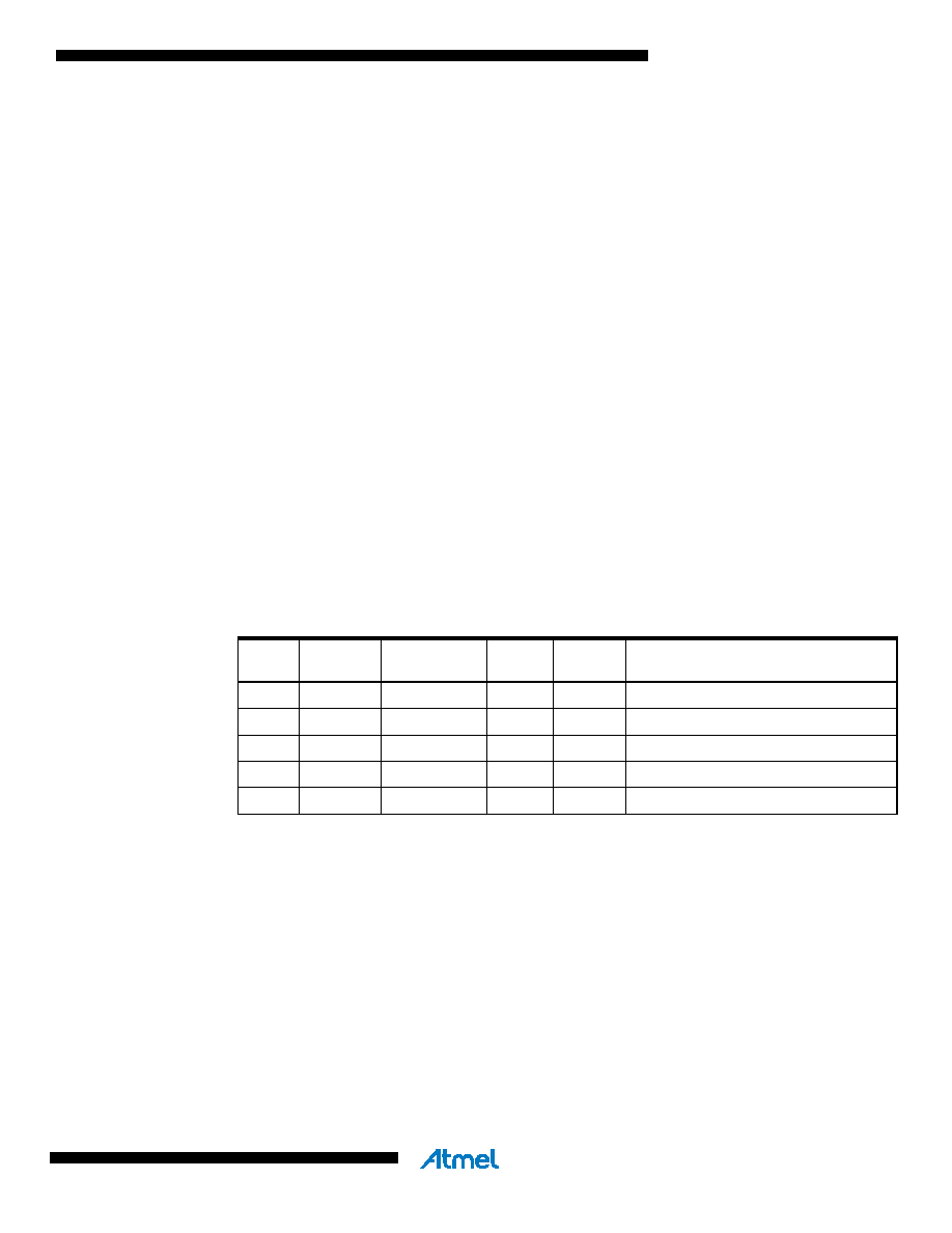
Table 10-1 summarizes the control signals for the pin value.
10.1.4
Reading the Pin Value
Independent of the setting of Data Direction bit DDxn, the port pin can be read through the
PINxn Register bit. As shown in Figure 10-2, the PINxn Register bit and the preceding latch con-
stitute a synchronizer. This is needed to avoid metastability if the physical pin changes value
near the edge of the internal clock, but it also introduces a delay. Figure 10-3 shows a timing dia-
gram of the synchronization when reading an externally applied pin value. The maximum and
minimum propagation delays are denoted t
pd,max and tpd,min respectively.
Table 10-1.
Port Pin Configurations
DDxn
PORTxn
PUD
(in MCUCR)
I/O
Pull-up
Comment
0
X
Input
No
Tri-state (Hi-Z)
0
1
0
Input
Yes
Pxn will source current if ext. pulled low
0
1
Input
No
Tri-state (Hi-Z)
1
0
X
Output
No
Output Low (Sink)
1
X
Output
No
Output High (Source)
相关PDF资料 |
PDF描述 |
|---|---|
| R5F2L3ACCNFP | 8-BIT, FLASH, 20 MHz, MICROCONTROLLER, PQFP100 |
| R5F2L38ACNFA | 8-BIT, FLASH, 20 MHz, MICROCONTROLLER, PQFP80 |
| R5F2L38CCNFP | 8-BIT, FLASH, 20 MHz, MICROCONTROLLER, PQFP80 |
| R5F2L387CDFP | 8-BIT, FLASH, 20 MHz, MICROCONTROLLER, PQFP80 |
| R5F2L387CNFP | 8-BIT, FLASH, 20 MHz, MICROCONTROLLER, PQFP80 |
相关代理商/技术参数 |
参数描述 |
|---|---|
| R5F2L3AACDFP#U1 | 制造商:Renesas Electronics Corporation 功能描述: |
| R5F2L3AACDFP#V0 | 制造商:Renesas Electronics Corporation 功能描述:R8C/L3AC 96K+4K/10K 100LQFP14X14 -40-+85 - Trays |
| R5F2L3AACNFA#U0 | 制造商:Renesas Electronics Corporation 功能描述:R8CL3AC 96+4KB 1.8/5.5V -20 TO 85C 100QFP - Trays 制造商:Renesas Electronics Corporation 功能描述:IC MCU 16BIT 96KB FLASH 100LQFP |
| R5F2L3AACNFP#30 | 制造商:Renesas Electronics Corporation 功能描述:IC MCU 16BIT 96KB FLASH 100LQFP 制造商:Renesas Electronics Corporation 功能描述:R8C Series 16 bit 10 kB RAM 96 kB Flash Single Chip Microcontroller SMT-LQFP-100 |
| R5F2L3AACNFP#V0 | 功能描述:MCU 1KB FLASH 96K ROM 100-LQFP RoHS:是 类别:集成电路 (IC) >> 嵌入式 - 微控制器, 系列:R8C/Lx/3AC 标准包装:250 系列:56F8xxx 核心处理器:56800E 芯体尺寸:16-位 速度:60MHz 连通性:CAN,SCI,SPI 外围设备:POR,PWM,温度传感器,WDT 输入/输出数:21 程序存储器容量:40KB(20K x 16) 程序存储器类型:闪存 EEPROM 大小:- RAM 容量:6K x 16 电压 - 电源 (Vcc/Vdd):2.25 V ~ 3.6 V 数据转换器:A/D 6x12b 振荡器型:内部 工作温度:-40°C ~ 125°C 封装/外壳:48-LQFP 包装:托盘 配用:MC56F8323EVME-ND - BOARD EVALUATION MC56F8323 |
发布紧急采购,3分钟左右您将得到回复。