- 您现在的位置:买卖IC网 > PDF目录69312 > R5F2L3AACDFP 8-BIT, FLASH, 20 MHz, MICROCONTROLLER, PQFP100 PDF资料下载
参数资料
| 型号: | R5F2L3AACDFP |
| 元件分类: | 微控制器/微处理器 |
| 英文描述: | 8-BIT, FLASH, 20 MHz, MICROCONTROLLER, PQFP100 |
| 封装: | 14 X 14 MM, 0.50 MM PITCH, PLASTIC, LQFP-100 |
| 文件页数: | 71/74页 |
| 文件大小: | 959K |
| 代理商: | R5F2L3AACDFP |
第1页第2页第3页第4页第5页第6页第7页第8页第9页第10页第11页第12页第13页第14页第15页第16页第17页第18页第19页第20页第21页第22页第23页第24页第25页第26页第27页第28页第29页第30页第31页第32页第33页第34页第35页第36页第37页第38页第39页第40页第41页第42页第43页第44页第45页第46页第47页第48页第49页第50页第51页第52页第53页第54页第55页第56页第57页第58页第59页第60页第61页第62页第63页第64页第65页第66页第67页第68页第69页第70页当前第71页第72页第73页第74页
74
2588F–AVR–06/2013
ATtiny261/461/861
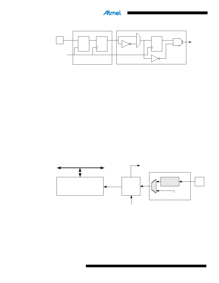
Figure 11-3.
T0 Pin Sampling
The synchronization and edge detector logic introduces a delay of 2.5 to 3.5 system clock cycles
from an edge has been applied to the T0 pin to the counter is updated.
Enabling and disabling of the clock input must be done when T0 has been stable for at least one
system clock cycle, otherwise it is a risk that a false Timer/Counter clock pulse is generated.
Each half period of the external clock applied must be longer than one system clock cycle to
ensure correct sampling. The external clock must be guaranteed to have less than half the sys-
tem clock frequency (f
ExtClk < fclk_I/O/2) given a 50/50% duty cycle. Since the edge detector uses
sampling, the maximum frequency of an external clock it can detect is half the sampling fre-
quency (Nyquist sampling theorem). However, due to variation of the system clock frequency
and duty cycle caused by Oscillator source (crystal, resonator, and capacitors) tolerances, it is
recommended that maximum frequency of an external clock source is less than f
clk_I/O/2.5.
An external clock source can not be prescaled.
11.4
Counter Unit
The main part of the 8-bit Timer/Counter is the programmable bi-directional counter unit. Figure
11-4 shows a block diagram of the counter and its surroundings.
Table 11-2.
Counter Unit Block Diagram
Signal description (internal signals):
count
Increment or decrement TCNT0 by 1.
clk
Tn
Timer/Counter clock, referred to as clk
T0 in the following.
top
Signalize that TCNT0 has reached maximum value.
The counter is incremented at each timer clock (clk
T0) until it passes its TOP value and then
restarts from BOTTOM. The counting sequence is determined by the setting of the CTC0 bit
located in the Timer/Counter Control Register (TCCR0A). For more details about counting
sequences, see “Modes of Operation” on page 77. clk
T0 can be generated from an external or
Tn_sync
(To Clock
Select Logic)
Edge Detector
Synchronization
DQ
LE
DQ
Tn
clk
I/O
DATA BUS
TCNTn
Control Logic
count
TOVn
(Int.Req.)
Clock Select
top
Tn
Edge
Detector
( From Prescaler )
clk
Tn
相关PDF资料 |
PDF描述 |
|---|---|
| R5F2L3ACCNFP | 8-BIT, FLASH, 20 MHz, MICROCONTROLLER, PQFP100 |
| R5F2L38ACNFA | 8-BIT, FLASH, 20 MHz, MICROCONTROLLER, PQFP80 |
| R5F2L38CCNFP | 8-BIT, FLASH, 20 MHz, MICROCONTROLLER, PQFP80 |
| R5F2L387CDFP | 8-BIT, FLASH, 20 MHz, MICROCONTROLLER, PQFP80 |
| R5F2L387CNFP | 8-BIT, FLASH, 20 MHz, MICROCONTROLLER, PQFP80 |
相关代理商/技术参数 |
参数描述 |
|---|---|
| R5F2L3AACDFP#U1 | 制造商:Renesas Electronics Corporation 功能描述: |
| R5F2L3AACDFP#V0 | 制造商:Renesas Electronics Corporation 功能描述:R8C/L3AC 96K+4K/10K 100LQFP14X14 -40-+85 - Trays |
| R5F2L3AACNFA#U0 | 制造商:Renesas Electronics Corporation 功能描述:R8CL3AC 96+4KB 1.8/5.5V -20 TO 85C 100QFP - Trays 制造商:Renesas Electronics Corporation 功能描述:IC MCU 16BIT 96KB FLASH 100LQFP |
| R5F2L3AACNFP#30 | 制造商:Renesas Electronics Corporation 功能描述:IC MCU 16BIT 96KB FLASH 100LQFP 制造商:Renesas Electronics Corporation 功能描述:R8C Series 16 bit 10 kB RAM 96 kB Flash Single Chip Microcontroller SMT-LQFP-100 |
| R5F2L3AACNFP#V0 | 功能描述:MCU 1KB FLASH 96K ROM 100-LQFP RoHS:是 类别:集成电路 (IC) >> 嵌入式 - 微控制器, 系列:R8C/Lx/3AC 标准包装:250 系列:56F8xxx 核心处理器:56800E 芯体尺寸:16-位 速度:60MHz 连通性:CAN,SCI,SPI 外围设备:POR,PWM,温度传感器,WDT 输入/输出数:21 程序存储器容量:40KB(20K x 16) 程序存储器类型:闪存 EEPROM 大小:- RAM 容量:6K x 16 电压 - 电源 (Vcc/Vdd):2.25 V ~ 3.6 V 数据转换器:A/D 6x12b 振荡器型:内部 工作温度:-40°C ~ 125°C 封装/外壳:48-LQFP 包装:托盘 配用:MC56F8323EVME-ND - BOARD EVALUATION MC56F8323 |
发布紧急采购,3分钟左右您将得到回复。