- 您现在的位置:买卖IC网 > PDF目录11680 > R5F56217BDLE#U0 (Renesas Electronics America)MCU 32BIT FLASH 384KROM 145TFLGA PDF资料下载
参数资料
| 型号: | R5F56217BDLE#U0 |
| 厂商: | Renesas Electronics America |
| 文件页数: | 75/148页 |
| 文件大小: | 0K |
| 描述: | MCU 32BIT FLASH 384KROM 145TFLGA |
| 产品培训模块: | RX Compare Match Timer RX DMAC |
| 标准包装: | 1 |
| 系列: | RX600 |
| 核心处理器: | RX |
| 芯体尺寸: | 32-位 |
| 速度: | 100MHz |
| 连通性: | CAN,EBI/EMI,I²C,SCI,SPI,USB |
| 外围设备: | DMA,LVD,POR,PWM,WDT |
| 输入/输出数: | 103 |
| 程序存储器容量: | 384KB(384K x 8) |
| 程序存储器类型: | 闪存 |
| RAM 容量: | 64K x 8 |
| 电压 - 电源 (Vcc/Vdd): | 2.7 V ~ 3.6 V |
| 数据转换器: | A/D 8x10/12b,D/A 2x10b |
| 振荡器型: | 内部 |
| 工作温度: | -40°C ~ 85°C |
| 封装/外壳: | 145-TFLGA |
| 包装: | 托盘 |
第1页第2页第3页第4页第5页第6页第7页第8页第9页第10页第11页第12页第13页第14页第15页第16页第17页第18页第19页第20页第21页第22页第23页第24页第25页第26页第27页第28页第29页第30页第31页第32页第33页第34页第35页第36页第37页第38页第39页第40页第41页第42页第43页第44页第45页第46页第47页第48页第49页第50页第51页第52页第53页第54页第55页第56页第57页第58页第59页第60页第61页第62页第63页第64页第65页第66页第67页第68页第69页第70页第71页第72页第73页第74页当前第75页第76页第77页第78页第79页第80页第81页第82页第83页第84页第85页第86页第87页第88页第89页第90页第91页第92页第93页第94页第95页第96页第97页第98页第99页第100页第101页第102页第103页第104页第105页第106页第107页第108页第109页第110页第111页第112页第113页第114页第115页第116页第117页第118页第119页第120页第121页第122页第123页第124页第125页第126页第127页第128页第129页第130页第131页第132页第133页第134页第135页第136页第137页第138页第139页第140页第141页第142页第143页第144页第145页第146页第147页第148页
PIC18F6520/8520/6620/8620/6720/8720
DS39609B-page 30
2004 Microchip Technology Inc.
3.1
Power-on Reset (POR)
A Power-on Reset pulse is generated on-chip when
VDD rise is detected. To take advantage of the POR
circuitry, tie the MCLR pin through a 1 k
to 10 k
resistor to VDD. This will eliminate external RC
components usually needed to create a Power-on
Reset delay. A minimum rise rate for VDD is specified
(parameter D004). For a slow rise time, see Figure 3-2.
When the device starts normal operation (i.e., exits the
Reset condition), device operating parameters (volt-
age, frequency, temperature, etc.) must be met to
ensure operation. If these conditions are not met, the
device must be held in Reset until the operating
conditions are met.
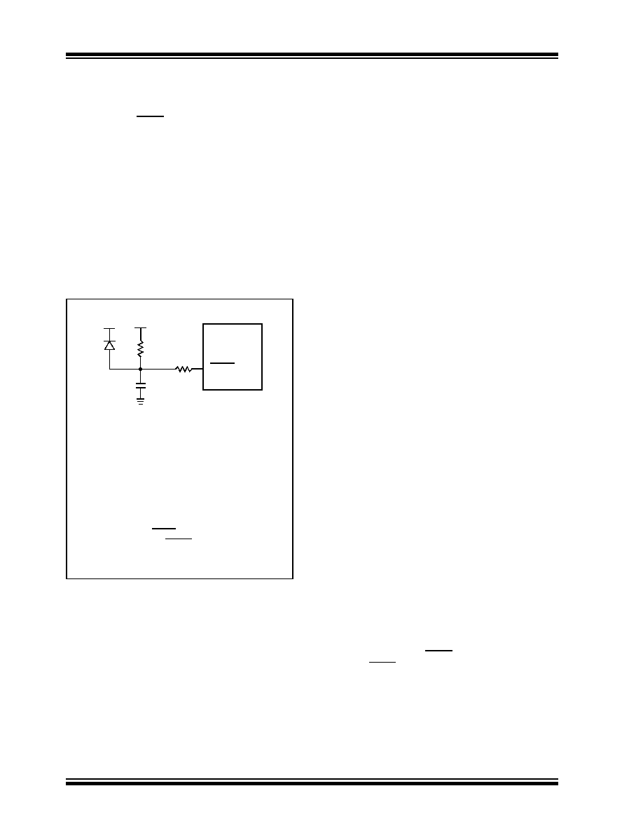
FIGURE 3-2:
EXTERNAL POWER-ON
RESET CIRCUIT (FOR
SLOW VDD POWER-UP)
3.2
Power-up Timer (PWRT)
The Power-up Timer provides a fixed nominal time-out
(parameter #33) only on power-up from the POR. The
Power-up Timer operates on an internal RC oscillator.
The chip is kept in Reset as long as the PWRT is active.
The PWRT’s time delay allows VDD to rise to an accept-
able level. A configuration bit is provided to enable/
disable the PWRT.
The power-up time delay will vary from chip-to-chip due
to VDD, temperature and process variation. See DC
parameter #33 for details.
3.3
Oscillator Start-up Timer (OST)
The Oscillator Start-up Timer (OST) provides 1024
oscillator cycles (from OSC1 input) delay after the
PWRT delay is over (parameter #32). This ensures that
the crystal oscillator or resonator has started and
stabilized.
The OST time-out is invoked only for XT, LP and HS
modes and only on Power-on Reset, or wake-up from
Sleep.
3.4
PLL Lock Time-out
With the PLL enabled, the time-out sequence following
a Power-on Reset is different from other oscillator
modes. A portion of the Power-up Timer is used to
provide a fixed time-out that is sufficient for the PLL to
lock to the main oscillator frequency. This PLL lock
time-out (TPLL) is typically 2 ms and follows the
oscillator start-up time-out.
3.5
Brown-out Reset (BOR)
A configuration bit, BOREN, can disable (if clear/
programmed), or enable (if set) the Brown-out Reset
circuitry. If VDD falls below parameter D005 for greater
than parameter #35, the brown-out situation will reset
the chip. A Reset may not occur if VDD falls below
parameter D005 for less than parameter #35. The chip
will remain in Brown-out Reset until VDD rises above
BVDD. If the Power-up Timer is enabled, it will be
invoked after VDD rises above BVDD; it then will keep
the chip in Reset for an additional time delay (parame-
ter #33). If VDD drops below BVDD while the Power-up
Timer is running, the chip will go back into a Brown-out
Reset and the Power-up Timer will be initialized. Once
VDD rises above BVDD, the Power-up Timer will
execute the additional time delay.
3.6
Time-out Sequence
On power-up, the time-out sequence is as follows:
First, PWRT time-out is invoked after the POR time
delay has expired. Then, OST is activated. The total
time-out will vary based on oscillator configuration and
the status of the PWRT. For example, in RC mode with
the PWRT disabled, there will be no time-out at all.
power-up.
Since the time-outs occur from the POR pulse, the
time-outs will expire if MCLR is kept low long enough.
Bringing MCLR high will begin execution immediately
(Figure 3-5). This is useful for testing purposes, or to
synchronize more than one PIC18FXX20 device
operating in parallel.
Table 3-2 shows the Reset conditions for some Special
Function Registers, while Table 3-3 shows the Reset
conditions for all of the registers.
Note 1:
External Power-on Reset circuit is required
only if the VDD power-up slope is too slow.
The diode D helps discharge the capacitor
quickly when VDD powers down.
2:
R < 40 k
is recommended to make sure that
the voltage drop across R does not violate
the device’s electrical specification.
3:
R1 = 1 k
to 10 k will limit any current flow-
ing into MCLR from external capacitor C, in
the event of MCLR/VPP pin breakdown due to
Electrostatic Discharge (ESD) or Electrical
Overstress (EOS).
C
R1
R
D
VDD
MCLR
PIC18FXX20
相关PDF资料 |
PDF描述 |
|---|---|
| D38999/24MD97SN | CONN RCPT 12POS JAM NUT W/SCKT |
| MS27656E23B21S | CONN RCPT 21POS WALL MNT W/SCKT |
| D38999/26FE99SB | CONN PLUG 23POS STRAIGHT W/SCKT |
| D38999/24MF11PN | CONN RCPT 11POS JAM NUT W/PINS |
| D38999/24WD97JN | CONN RCPT 12POS JAM NUT W/SCKT |
相关代理商/技术参数 |
参数描述 |
|---|---|
| R5F56218BDBG | 制造商:Renesas Electronics Corporation 功能描述:MCU 32BIT RX621 176BGA |
| R5F56218BDBG#U0 | 功能描述:MCU 32BIT FLASH 512KROM 176LFBGA RoHS:是 类别:集成电路 (IC) >> 嵌入式 - 微控制器, 系列:RX600 标准包装:96 系列:PIC® 16F 核心处理器:PIC 芯体尺寸:8-位 速度:20MHz 连通性:I²C,SPI 外围设备:欠压检测/复位,POR,PWM,WDT 输入/输出数:11 程序存储器容量:3.5KB(2K x 14) 程序存储器类型:闪存 EEPROM 大小:- RAM 容量:128 x 8 电压 - 电源 (Vcc/Vdd):2.3 V ~ 5.5 V 数据转换器:A/D 8x10b 振荡器型:内部 工作温度:-40°C ~ 125°C 封装/外壳:14-TSSOP(0.173",4.40mm 宽) 包装:管件 |
| R5F56218BDFB | 制造商:Renesas Electronics Corporation 功能描述:MCU 32BIT RX621 144QFP |
| R5F56218BDFB#V0 | 功能描述:MCU 32BIT FLASH 512K ROM 144LQFP RoHS:是 类别:集成电路 (IC) >> 嵌入式 - 微控制器, 系列:RX600 标准包装:96 系列:PIC® 16F 核心处理器:PIC 芯体尺寸:8-位 速度:20MHz 连通性:I²C,SPI 外围设备:欠压检测/复位,POR,PWM,WDT 输入/输出数:11 程序存储器容量:3.5KB(2K x 14) 程序存储器类型:闪存 EEPROM 大小:- RAM 容量:128 x 8 电压 - 电源 (Vcc/Vdd):2.3 V ~ 5.5 V 数据转换器:A/D 8x10b 振荡器型:内部 工作温度:-40°C ~ 125°C 封装/外壳:14-TSSOP(0.173",4.40mm 宽) 包装:管件 |
| R5F56218BDFP | 制造商:Renesas Electronics Corporation 功能描述:MCU 32BIT RX621 100QFP |
发布紧急采购,3分钟左右您将得到回复。