- 您现在的位置:买卖IC网 > PDF目录225141 > S29WS128N0LBFI011 (Spansion Inc.) 256/128/64 MEGABIT CMOS 1.8 VOLT ONLY SIMULTANEOUS READ/WRITE BURST MODE FLASH MEMORY PDF资料下载
参数资料
| 型号: | S29WS128N0LBFI011 |
| 厂商: | Spansion Inc. |
| 英文描述: | 256/128/64 MEGABIT CMOS 1.8 VOLT ONLY SIMULTANEOUS READ/WRITE BURST MODE FLASH MEMORY |
| 中文描述: | 256/128/64兆位的CMOS 1.8伏只有同时读/写突发模式闪存 |
| 文件页数: | 91/99页 |
| 文件大小: | 1091K |
| 代理商: | S29WS128N0LBFI011 |
第1页第2页第3页第4页第5页第6页第7页第8页第9页第10页第11页第12页第13页第14页第15页第16页第17页第18页第19页第20页第21页第22页第23页第24页第25页第26页第27页第28页第29页第30页第31页第32页第33页第34页第35页第36页第37页第38页第39页第40页第41页第42页第43页第44页第45页第46页第47页第48页第49页第50页第51页第52页第53页第54页第55页第56页第57页第58页第59页第60页第61页第62页第63页第64页第65页第66页第67页第68页第69页第70页第71页第72页第73页第74页第75页第76页第77页第78页第79页第80页第81页第82页第83页第84页第85页第86页第87页第88页第89页第90页当前第91页第92页第93页第94页第95页第96页第97页第98页第99页
January 25, 2005 S29WS-N_00_G0
89
Ad vance
Information
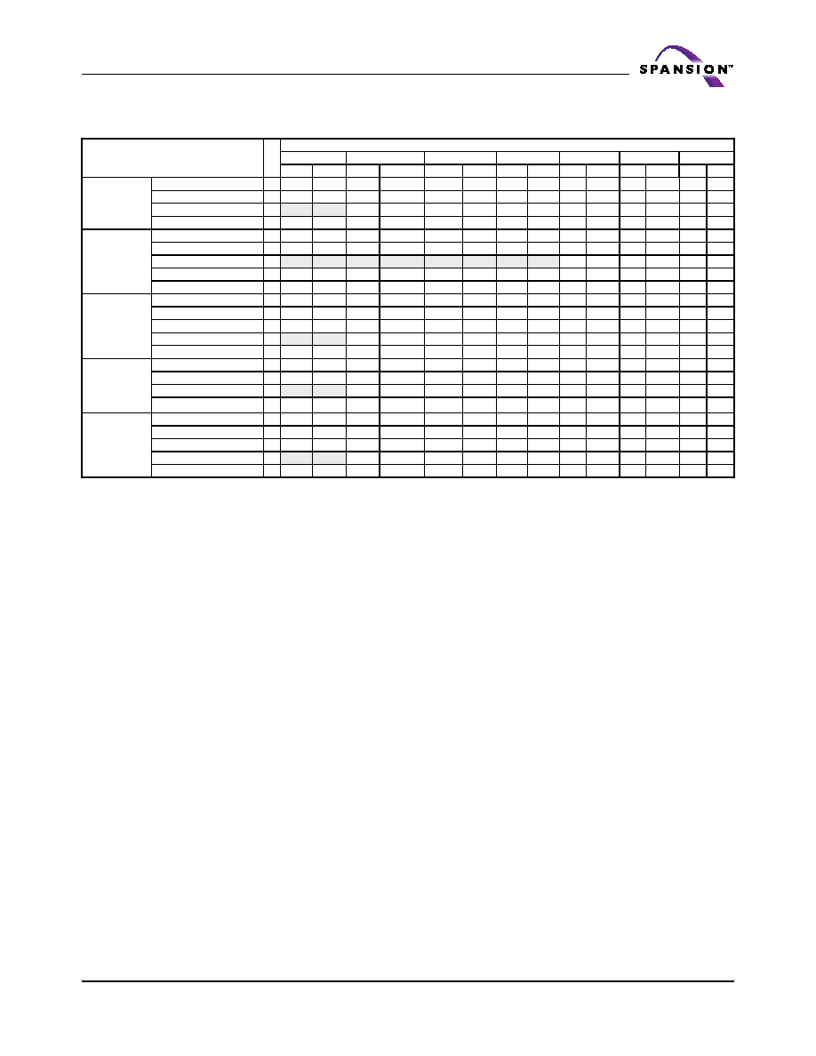
Table 12.2. Sector Protection Commands
Command Sequence
(Notes)
Cy
cl
es
Bus Cycles (Notes 1–4)
First
Second
Third
Fourth
Fifth
Sixth
Seventh
Addr
Data
Addr
Data
Addr
Data
Addr
Data Addr Data Addr Data Addr Data
Lock
Register
Bits
Command Set Entry (5)
3
555
AA
2AA
55
555
40
2
XX
A0
77/00
data
Read (6)
1
77
data
Command Set Exit (7)
2
XX
90
XX
00
Password
Protection
Command Set Entry (5)
3
555
AA
2AA
55
555
60
Program [0-3] (8)
2
XX
A0
00
PWD[0-3]
Read (9)
4 0...00 PWD0 0...01
PWD1
0...02
PWD2 0...03 PWD3
Unlock
7
00
25
00
03
00
PWD0
01
PWD1
02
PWD2
03
PWD3
00
29
Command Set Exit (7)
2
XX
90
XX
00
Non-Volatile
Sector
Protection (PPB)
Command Set Entry (5)
3
555
AA
2AA
55
[BA]555
C0
PPB Program (10)
2
XX
A0
SA
00
All PPB Erase (10, 11)
2
XX
80
00
30
PPB Status Read
1
SA
RD(0)
Command Set Exit (7)
2
XX
90
XX
00
Global
Volatile Sector
Protection
Freeze
(PPB Lock)
Command Set Entry (5)
3
555
AA
2AA
55
[BA]555
50
PPB Lock Bit Set
2
XX
A0
XX
00
PPB Lock Bit Status Read
1
BA
RD(0)
Command Set Exit (7)
2
XX
90
XX
00
Volatile Sector
Protection
(DYB)
Command Set Entry (5)
3
555
AA
2AA
55
[BA]555
E0
DYB Set
2
XX
A0
SA
00
DYB Clear
2
XX
A0
SA
01
DYB Status Read
1
SA
RD(0)
Command Set Exit (7)
2
XX
90
XX
00
Legend:
X = Don’t care.
RA = Address of the memory location to be read.
PD(0) = SecSi Sector Lock Bit. PD(0), or bit[0].
PD(1) = Persistent Protection Mode Lock Bit. PD(1), or bit[1], must
be set to ‘0’ for protection while PD(2), bit[2] must be left as ‘1’.
PD(2) = Password Protection Mode Lock Bit. PD(2), or bit[2], must
be set to ‘0’ for protection while PD(1), bit[1] must be left as ‘1’.
PD(3) = Protection Mode OTP Bit. PD(3) or bit[3].
SA = Sector Address. WS256N = A23–A14; WS128N = A22–A14;
WS064N = A21–A14.
BA = Bank Address. WS256N = A23–A20; WS128N = A22–A20;
WS064N = A21–A18.
PWD3–PWD0 = Password Data. PD3–PD0 present four 16 bit
combinations that represent the 64-bit Password
PWA = Password Address. Address bits A1 and A0 are used to select
each 16-bit portion of the 64-bit entity.
PWD = Password Data.
RD(0), RD(1), RD(2) = DQ0, DQ1, or DQ2 protection indicator bit. If
protected, DQ0, DQ1, or DQ2 = 0. If unprotected, DQ0, DQ1,
DQ2 = 1.
Notes:
1. All values are in hexadecimal.
2. Shaded cells indicate read cycles.
3. Address and data bits not specified in table, legend, or notes are
don’t cares (each hex digit implies 4 bits of data).
4. Writing incorrect address and data values or writing them in the
improper sequence may place the device in an unknown state.
The system must write the reset command to return the device
to reading array data.
5. Entry commands are required to enter a specific mode to enable
instructions only available within that mode.
6. If both the Persistent Protection Mode Locking Bit and the
Password Protection Mode Locking Bit are set at the same time,
the command operation aborts and returns the device to the
default Persistent Sector Protection Mode during 2nd bus cycle.
Note that on all future devices, addresses equal 00h, but is
explanation of lock bits.
7. Exit command must be issued to reset the device into read
mode; device may otherwise be placed in an unknown state.
8. Entire two bus-cycle sequence must be entered for each portion
of the password.
9. Full address range is required for reading password.
10. See Figure 8.2 for details.
11. “All PPB Erase” command pre-programs all PPBs before erasure
to prevent over-erasure.
12. The second cycle address for the lock register program operation
is 77 for S29Ws256N; however, for WS128N and Ws064N this
address is 00.
相关PDF资料 |
PDF描述 |
|---|---|
| S29WS128N0LBFI012 | 256/128/64 MEGABIT CMOS 1.8 VOLT ONLY SIMULTANEOUS READ/WRITE BURST MODE FLASH MEMORY |
| S29WS128N0LBFI013 | 256/128/64 MEGABIT CMOS 1.8 VOLT ONLY SIMULTANEOUS READ/WRITE BURST MODE FLASH MEMORY |
| S29WS128N0LBFI110 | 256/128/64 MEGABIT CMOS 1.8 VOLT ONLY SIMULTANEOUS READ/WRITE BURST MODE FLASH MEMORY |
| S29WS128N0LBFW010 | 256/128/64 MEGABIT CMOS 1.8 VOLT ONLY SIMULTANEOUS READ/WRITE BURST MODE FLASH MEMORY |
| S29WS256N0PBAW011 | 256/128/64 MEGABIT CMOS 1.8 VOLT ONLY SIMULTANEOUS READ/WRITE BURST MODE FLASH MEMORY |
相关代理商/技术参数 |
参数描述 |
|---|---|
| S29WS128N0LBFI012 | 制造商:SPANSION 制造商全称:SPANSION 功能描述:256/128/64 MEGABIT CMOS 1.8 VOLT ONLY SIMULTANEOUS READ/WRITE BURST MODE FLASH MEMORY |
| S29WS128N0LBFI013 | 制造商:SPANSION 制造商全称:SPANSION 功能描述:256/128/64 Megabit (16/8/4 M x 16-Bit) CMOS 1.8 Volt-only Simultaneous Read/Write, Burst Mode Flash Memory |
| S29WS128N0LBFI110 | 制造商:SPANSION 制造商全称:SPANSION 功能描述:256/128/64 MEGABIT CMOS 1.8 VOLT ONLY SIMULTANEOUS READ/WRITE BURST MODE FLASH MEMORY |
| S29WS128N0LBFI111 | 制造商:SPANSION 制造商全称:SPANSION 功能描述:256/128/64 MEGABIT CMOS 1.8 VOLT ONLY SIMULTANEOUS READ/WRITE BURST MODE FLASH MEMORY |
| S29WS128N0LBFI112 | 制造商:SPANSION 制造商全称:SPANSION 功能描述:256/128/64 MEGABIT CMOS 1.8 VOLT ONLY SIMULTANEOUS READ/WRITE BURST MODE FLASH MEMORY |
发布紧急采购,3分钟左右您将得到回复。