- 您现在的位置:买卖IC网 > PDF目录270895 > S29WS256N0PBAW010 (SPANSION LLC) 256/128/64 MEGABIT CMOS 1.8 VOLT ONLY SIMULTANEOUS READ/WRITE BURST MODE FLASH MEMORY PDF资料下载
参数资料
| 型号: | S29WS256N0PBAW010 |
| 厂商: | SPANSION LLC |
| 元件分类: | PROM |
| 英文描述: | 256/128/64 MEGABIT CMOS 1.8 VOLT ONLY SIMULTANEOUS READ/WRITE BURST MODE FLASH MEMORY |
| 中文描述: | 16M X 16 FLASH 1.8V PROM, 70 ns, PBGA84 |
| 封装: | 11.60 X 8 MM, LEAD FREE, PLASTIC, FBGA-84 |
| 文件页数: | 14/95页 |
| 文件大小: | 1745K |
| 代理商: | S29WS256N0PBAW010 |
第1页第2页第3页第4页第5页第6页第7页第8页第9页第10页第11页第12页第13页当前第14页第15页第16页第17页第18页第19页第20页第21页第22页第23页第24页第25页第26页第27页第28页第29页第30页第31页第32页第33页第34页第35页第36页第37页第38页第39页第40页第41页第42页第43页第44页第45页第46页第47页第48页第49页第50页第51页第52页第53页第54页第55页第56页第57页第58页第59页第60页第61页第62页第63页第64页第65页第66页第67页第68页第69页第70页第71页第72页第73页第74页第75页第76页第77页第78页第79页第80页第81页第82页第83页第84页第85页第86页第87页第88页第89页第90页第91页第92页第93页第94页第95页
October 29, 2004 S29WSxxxN_00_F0
21
Pre l i m i n a r y
The device outputs subsequent words tBACC after the active edge of each successive clock cy-
cle, which also increments the internal address counter. The device outputs burst data at this
rate subject to the following operational conditions:
starting address: whether the address is divisible by four (where A[1:0] is 00). A divisi-
ble-by-four address incurs the least number of additional wait states that occur after the
initial word. The number of additional wait states required increases for burst operations
in which the starting address is one, two, or three locations above the divisible-by-four
address (i.e., where A[1:0] is 01, 10, or 11).
boundary crossing: a physical aspect of the device that exists every 128 words, starting
at address 00007Fh. Higher operational speeds require one additional wait state. Refer to
Tables 7.10–7.13 for details. Figure 11.20 shows the effects of boundary crossings at
higher frequencies.
clock frequency: the speed at which the device is expected to burst data. Higher speeds
show the effects of frequency on burst operation.
In all cases, with or without latency, the RDY output indicates when the next data is available
to be read.
Table 7.5 shows the latency that occurs in the S29WS256N device when (x indicates the rec-
ommended number of wait states for various operating frequencies, as shown in Table 7.15,
configuration register bits CR13-CR11).
frequency, and wait state setting (configuration register bits CR13–CR11) for the S29WS128N
and S29WS064N devices. Tables 7.10–7.13 includes the wait state that occurs when crossing
the internal boundary.
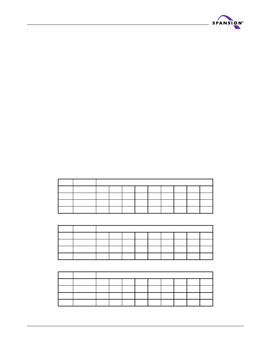
Table 7.5. Address Latency for x Wait States (
≤ 80 MHz, WS256N only)
Table 7.6. Address Latency for 6 Wait States (
≤ 80 MHz)
Table 7.7. Address Latency for 5 Wait States (
≤ 68 MHz)
Word
Wait States
Cycle
0
x ws
D0
D1
D2
D3
D4
D5
D6
D7
D8
1
x ws
D1
D2
D3
1 ws
D4
D5
D6
D7
D8
2
x ws
D2
D3
1 ws
D4
D5
D6
D7
D8
3
x ws
D3
1 ws
D4
D5
D6
D7
D8
Word
Wait States
Cycle
0
6 ws
D0
D1
D2
D3
D4
D5
D6
D7
D8
1
6 ws
D1
D2
D3
1 ws
D4
D5
D6
D7
D8
2
6 ws
D2
D3
1 ws
D4
D5
D6
D7
D8
3
6 ws
D3
1 ws
D4
D5
D6
D7
D8
Word
Wait States
Cycle
0
5 ws
D0
D1
D2
D3
D4
D5
D6
D7
D8
1
5 ws
D1
D2
D3
D4
D5
D6
D7
D8
D9
2
5 ws
D2
D3
1 ws
D4
D5
D6
D7
D8
D9
3
5 ws
D3
1 ws
D4
D5
D6
D7
D8
D9
相关PDF资料 |
PDF描述 |
|---|---|
| S29WS064N0PBAW010 | 256/128/64 MEGABIT CMOS 1.8 VOLT ONLY SIMULTANEOUS READ/WRITE BURST MODE FLASH MEMORY |
| S29GL256N90FFI013 | MirrorBit Flash Family |
| S29GL256N10FFI013 | MirrorBit Flash Family |
| S29AL016M90FFI013 | 16 MEGABIT (2M X 8 BIT / I M X 16 BIT) 3.0 VOLT ONLY BOOT SECTOR FLASH MEMORY |
| S29AL016M10FFI013 | 16 MEGABIT (2M X 8 BIT / I M X 16 BIT) 3.0 VOLT ONLY BOOT SECTOR FLASH MEMORY |
相关代理商/技术参数 |
参数描述 |
|---|---|
| S29WS256N0PBAW011 | 制造商:SPANSION 制造商全称:SPANSION 功能描述:256/128/64 MEGABIT CMOS 1.8 VOLT ONLY SIMULTANEOUS READ/WRITE BURST MODE FLASH MEMORY |
| S29WS256N0PBAW012 | 制造商:SPANSION 制造商全称:SPANSION 功能描述:256/128/64 Megabit (16/8/4 M x 16-Bit) CMOS 1.8 Volt-only Simultaneous Read/Write, Burst Mode Flash Memory |
| S29WS256N0PBAW013 | 制造商:SPANSION 制造商全称:SPANSION 功能描述:256/128/64 Megabit (16/8/4 M x 16-Bit) CMOS 1.8 Volt-only Simultaneous Read/Write, Burst Mode Flash Memory |
| S29WS256N0PBAW110 | 制造商:SPANSION 制造商全称:SPANSION 功能描述:256/128/64 MEGABIT CMOS 1.8 VOLT ONLY SIMULTANEOUS READ/WRITE BURST MODE FLASH MEMORY |
| S29WS256N0PBAW111 | 制造商:SPANSION 制造商全称:SPANSION 功能描述:256/128/64 MEGABIT CMOS 1.8 VOLT ONLY SIMULTANEOUS READ/WRITE BURST MODE FLASH MEMORY |
发布紧急采购,3分钟左右您将得到回复。