- 您现在的位置:买卖IC网 > PDF目录69327 > S80C188EB-13 (INTEL CORP) 16-BIT, 13 MHz, MICROPROCESSOR, PQFP80 PDF资料下载
参数资料
| 型号: | S80C188EB-13 |
| 厂商: | INTEL CORP |
| 元件分类: | 微控制器/微处理器 |
| 英文描述: | 16-BIT, 13 MHz, MICROPROCESSOR, PQFP80 |
| 封装: | EIAJ, QFP-80 |
| 文件页数: | 3/59页 |
| 文件大小: | 1928K |
| 代理商: | S80C188EB-13 |
第1页第2页当前第3页第4页第5页第6页第7页第8页第9页第10页第11页第12页第13页第14页第15页第16页第17页第18页第19页第20页第21页第22页第23页第24页第25页第26页第27页第28页第29页第30页第31页第32页第33页第34页第35页第36页第37页第38页第39页第40页第41页第42页第43页第44页第45页第46页第47页第48页第49页第50页第51页第52页第53页第54页第55页第56页第57页第58页第59页
80C186EB80C188EB 80L186EB80L188EB
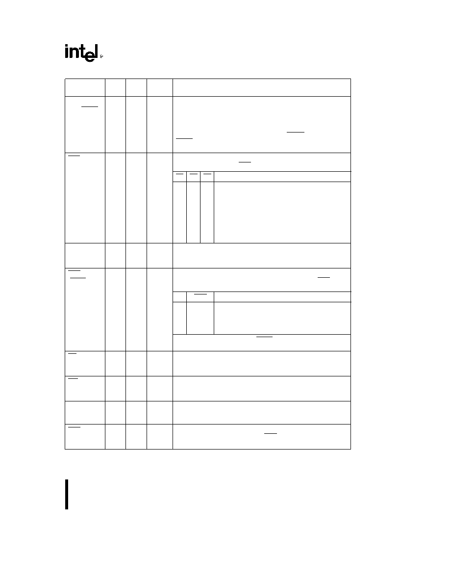
Table 3 Pin Descriptions
(Continued)
Pin
Input
Output
Description
Name
Type
States
A1816
IO
A(L)
H(Z)
These pins provide multiplexed Address during the address
phase of the bus cycle Address bits 16 through 19 are presented
A19ONCE
R(WH)
on these pins and can be latched using ALE These pins are
(A15A8)
P(X)
driven to a logic 0 during the data phase of the bus cycle On the
(A1816)
80C188EB A15 – A8 provide valid address information for the
(A19ONCE)
entire bus cycle During a processor reset (RESIN active) A19
ONCE is used to enable ONCE mode A1816 must not be driven
low during reset or improper operation may result
S20
O
H(Z)
Bus cycle Status are encoded on these pins to provide bus
transaction information S20 are encoded as follows
R(Z)
P(1)
S2
S1
S0
Bus Cycle Initiated
0
Interrupt Acknowledge
0
1
Read IO
0
1
0
Write IO
0
1
Processor HALT
1
0
Queue Instruction Fetch
1
0
1
Read Memory
1
0
Write Memory
1
Passive (no bus activity)
ALE
O
H(0)
Address Latch Enable
output is used to strobe address
information into a transparent type latch during the address phase
R(0)
of the bus cycle
P(0)
BHE
O
H(Z)
Byte High Enable
output to indicate that the bus cycle in progress
is transferring data over the upper half of the data bus BHE and
(RFSH)
R(Z)
A0 have the following logical encoding
P(X)
A0
BHE
Encoding
(for the 80C186EB80L186EB only)
0
Word Transfer
0
1
Even Byte Transfer
1
0
Odd Byte Transfer
1
Refresh Operation
On the 80C188EB80L188EB RFSH is asserted low to indicate a
refresh bus cycle
RD
O
H(Z)
ReaD
output signals that the accessed memory or IO device
must drive data information onto the data bus
R(Z)
P(1)
WR
O
H(Z)
WRite
output signals that data available on the data bus are to be
written into the accessed memory or IO device
R(Z)
P(1)
READY
I
A(L)
READY
input to signal the completion of a bus cycle READY
must be active to terminate any bus cycle unless it is ignored by
S(L)
correctly programming the Chip-Select Unit
DEN
O
H(Z)
Data ENable
output to control the enable of bi-directional
transceivers in a buffered system DEN is active only when data is
R(Z)
to be transferred on the bus
P(1)
NOTE
Pin names in parentheses apply to the 80C188EB80L188EB
11
相关PDF资料 |
PDF描述 |
|---|---|
| S80C188EB-20 | 16-BIT, 20 MHz, MICROPROCESSOR, PQFP80 |
| SB80C188EB-20 | 16-BIT, 20 MHz, MICROPROCESSOR, PQFP80 |
| SB80C188EB-25 | 16-BIT, 25 MHz, MICROPROCESSOR, PQFP80 |
| S80L186EB-13 | 16-BIT, 13 MHz, MICROPROCESSOR, PQFP80 |
| SB80L188EB-13 | 16-BIT, 13 MHz, MICROPROCESSOR, PQFP80 |
相关代理商/技术参数 |
参数描述 |
|---|---|
| S80C188EB20 | 制造商:INTEL 制造商全称:Intel Corporation 功能描述:16-BIT HIGH-INTEGRATION EMBEDDED PROCESSORS |
| S80C188EB25 | 功能描述:IC MPU 16-BIT 5V 25MHZ 80-MQFP RoHS:否 类别:集成电路 (IC) >> 嵌入式 - 微处理器 系列:- 标准包装:2 系列:MPC8xx 处理器类型:32-位 MPC8xx PowerQUICC 特点:- 速度:133MHz 电压:3.3V 安装类型:表面贴装 封装/外壳:357-BBGA 供应商设备封装:357-PBGA(25x25) 包装:托盘 |
| S80C188EB-25 | 制造商:未知厂家 制造商全称:未知厂家 功能描述:16-Bit Microprocessor |
| S80C188EC13 | 制造商:INTEL 制造商全称:Intel Corporation 功能描述:16-BIT HIGH-INTEGRATION EMBEDDED PROCESSORS |
| S80C188EC-13 | 制造商:未知厂家 制造商全称:未知厂家 功能描述:16-Bit Microprocessor |
发布紧急采购,3分钟左右您将得到回复。