- 您现在的位置:买卖IC网 > PDF目录98071 > S82451KX (INTEL CORP) SPECIALTY MICROPROCESSOR CIRCUIT, PQFP144 PDF资料下载
参数资料
| 型号: | S82451KX |
| 厂商: | INTEL CORP |
| 元件分类: | 微控制器/微处理器 |
| 英文描述: | SPECIALTY MICROPROCESSOR CIRCUIT, PQFP144 |
| 封装: | QFP-144 |
| 文件页数: | 6/180页 |
| 文件大小: | 1094K |
| 代理商: | S82451KX |
第1页第2页第3页第4页第5页当前第6页第7页第8页第9页第10页第11页第12页第13页第14页第15页第16页第17页第18页第19页第20页第21页第22页第23页第24页第25页第26页第27页第28页第29页第30页第31页第32页第33页第34页第35页第36页第37页第38页第39页第40页第41页第42页第43页第44页第45页第46页第47页第48页第49页第50页第51页第52页第53页第54页第55页第56页第57页第58页第59页第60页第61页第62页第63页第64页第65页第66页第67页第68页第69页第70页第71页第72页第73页第74页第75页第76页第77页第78页第79页第80页第81页第82页第83页第84页第85页第86页第87页第88页第89页第90页第91页第92页第93页第94页第95页第96页第97页第98页第99页第100页第101页第102页第103页第104页第105页第106页第107页第108页第109页第110页第111页第112页第113页第114页第115页第116页第117页第118页第119页第120页第121页第122页第123页第124页第125页第126页第127页第128页第129页第130页第131页第132页第133页第134页第135页第136页第137页第138页第139页第140页第141页第142页第143页第144页第145页第146页第147页第148页第149页第150页第151页第152页第153页第154页第155页第156页第157页第158页第159页第160页第161页第162页第163页第164页第165页第166页第167页第168页第169页第170页第171页第172页第173页第174页第175页第176页第177页第178页第179页第180页
PRELIMINARY
95
A
82453KX/GX, 82452KX/GX, 82451KX/GX (MC)
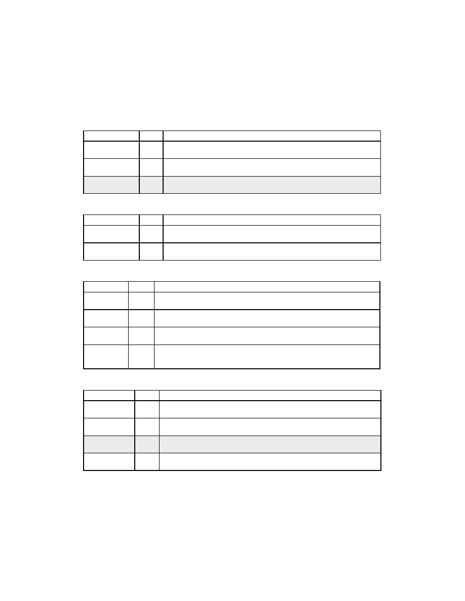
SYSCMD[4:0]#
O
CMOS
SYSTEM SIDE COMMAND. These signals send commands and other
information from the DC to the DP.
SYSDEN#
O
CMOS
SYSTEM SIDE DATA ENABLE. This signal permits the DC to control the
enabling of DP data information onto the host bus.
SYSERR#
I
CMOS
SYSTEM ERROR. This signal sends system error data conditions from the DP
to the DC.
Table 4. DC/MIC Interchip Signals (DC)
Signal
Type
Description
MICCMD[6:0]#
O
CMOS
MIC COMMAND. Sends read/write/configuration commands to the MIC.
MICMWC[1:0]#
O
CMOS
MIC MEMORY WRITE COMMAND (TWO COPIES). Instructs the MIC to drive
write data held in its internal buffers on the memory data bus.
Table 5. Reset and Error Signals (DC)
Signal
Type
Description
BINIT#
I/O
GTL+
BUS INITIALIZATION. BINIT# is asserted to initialize the host bus. Configuration
registers are not affected.
MIRST#
O
CMOS
MEMORY INTERFACE RESET. The DC uses this signal to reset the DP and MIC.
RESET#
I
GTL+
RESET. This is a hard reset to the DC. The DC sets its internal registers to their
default conditions and asserts the MIRST# to the DP and MICs.
SBCERR#
O
CMOS
SINGLE BIT CORRECTED ERROR. When SBC error reporting is enabled in the
MERRCMD or SERRCMD Register, this signal is asserted to indicate that a single
bit error was detected and corrected in the memory array.
Table 6. Clock, Power, and Support SIgnals (DC)
Signal
Type
Description
BCLK
I
CMOS
BUS CLOCK. This is the input clock for the DC.
GTLREFV
I
Analog
GTL REFERENCE VOLTAGE. GTLREFV sets the voltage level used by the GTL
input receivers for comparison against incoming GTL level signals.
OMCNUM
I
CMOS
MEMORY CONTROLLER NUMBER. During a power-on reset, this signal
provides the MC device number (see MCNUM Register).
PWRGD
I
CMOS
POWER GOOD. PWRGD is provided by the power supply when all voltages have
stabilized for at least 1 ms.
Table 3. DC/DP Interchip Signals (DC) (Continued)
Signal
Type
Description
相关PDF资料 |
PDF描述 |
|---|---|
| S83296SA | 16-BIT, MROM, 40 MHz, MICROCONTROLLER, PQFP100 |
| SB83296SA | 16-BIT, MROM, 40 MHz, MICROCONTROLLER, PQFP100 |
| S83C196MH | 16-BIT, MROM, 16 MHz, MICROCONTROLLER, PQFP80 |
| S83C51FB-BB44 | 8-BIT, MROM, 24 MHz, MICROCONTROLLER, PQFP44 |
| S83C51FC-5B44 | 8-BIT, MROM, 16 MHz, MICROCONTROLLER, PQFP44 |
相关代理商/技术参数 |
参数描述 |
|---|---|
| S82452KX | 制造商:未知厂家 制造商全称:未知厂家 功能描述:Data Path Controller |
| S82453KX | 制造商:未知厂家 制造商全称:未知厂家 功能描述:DRAM Controller |
| S82454KX | 制造商:未知厂家 制造商全称:未知厂家 功能描述:PCI Bus Interface/Controller |
| S8248P12NF | 功能描述:ANTENNA 824-896MHZ 8DBI N FML RoHS:是 类别:RF/IF 和 RFID >> RF 天线 系列:* 标准包装:1 系列:* |
| S82510 DIE | 制造商:Intel 功能描述: |
发布紧急采购,3分钟左右您将得到回复。