参数资料
| 型号: | SAA7706H/N210,518 |
| 厂商: | NXP Semiconductors |
| 文件页数: | 25/52页 |
| 文件大小: | 0K |
| 描述: | IC CAR RADIO DSP 80-QFP |
| 标准包装: | 500 |
| 类型: | 汽车信号处理器 |
| 接口: | I²C,I²:S,LSB,SPDIF |
| 电压 - 输入/输出: | 3.30V |
| 电压 - 核心: | 3.30V |
| 工作温度: | -40°C ~ 85°C |
| 安装类型: | 表面贴装 |
| 封装/外壳: | 80-BQFP |
| 供应商设备封装: | 80-QFP(14x20) |
| 包装: | 带卷 (TR) |
| 其它名称: | 935270285518 SAA7706H/N210-T SAA7706H/N210-T-ND |
第1页第2页第3页第4页第5页第6页第7页第8页第9页第10页第11页第12页第13页第14页第15页第16页第17页第18页第19页第20页第21页第22页第23页第24页当前第25页第26页第27页第28页第29页第30页第31页第32页第33页第34页第35页第36页第37页第38页第39页第40页第41页第42页第43页第44页第45页第46页第47页第48页第49页第50页第51页第52页
2001 Mar 05
31
Philips Semiconductors
Product specication
Car radio Digital Signal Processor (DSP)
SAA7706H
9I2C-BUS FORMAT
For more general information on the I2C-bus protocol, see
the Philips I2C-bus specification.
9.1
Addressing
Before any data is transmitted on the I2C-bus, the device
which should respond is addressed first. The addressing is
always done with the first byte transmitted after the start
procedure.
9.2
Slave address (pin A0)
The SAA7706H acts as slave receiver or a slave
transmitter. Therefore the clock signal SCL is only an input
signal. The data signal SDA is a bidirectional line. The
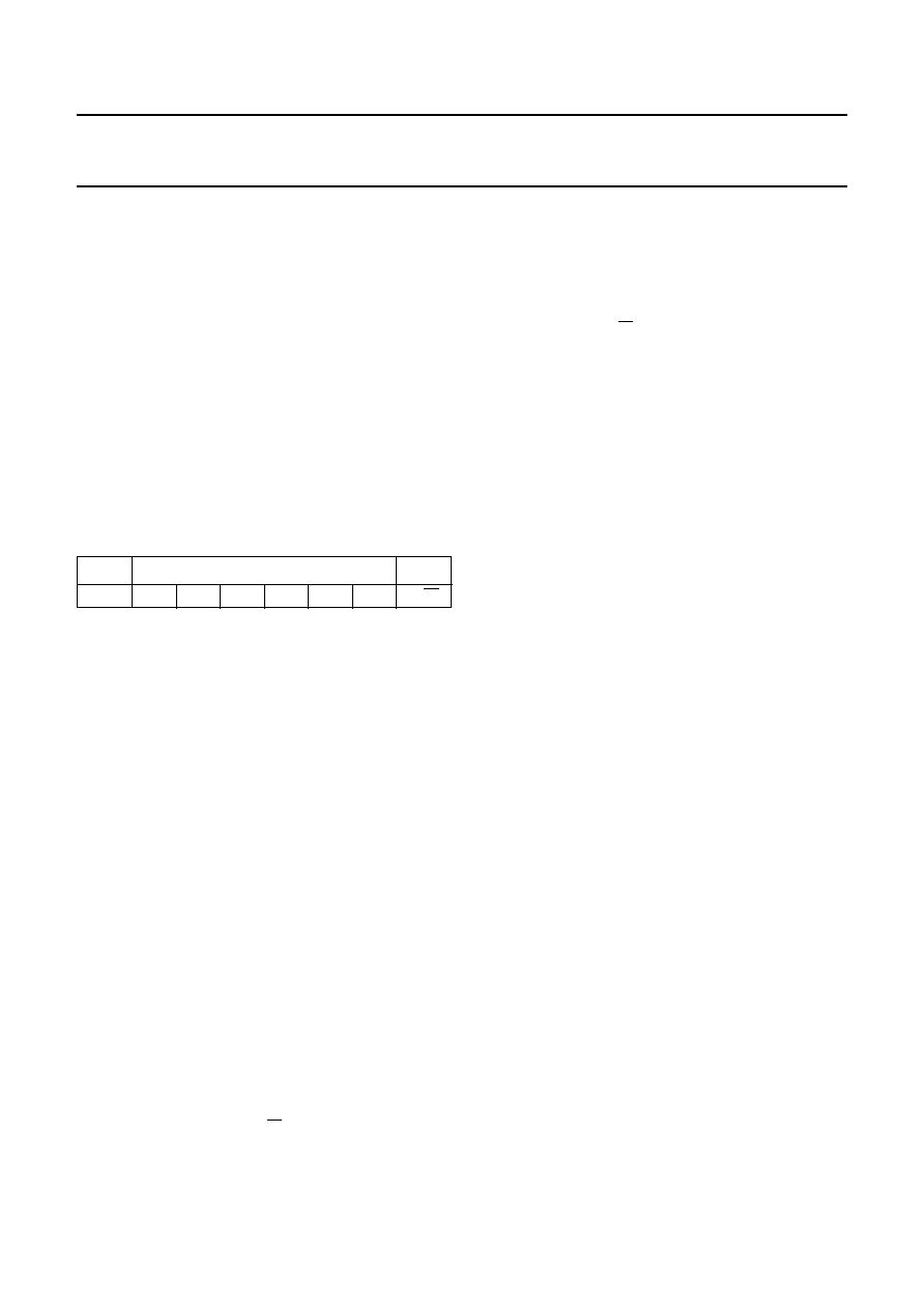
SAA7706H slave address is shown in Table 3.
Table 3
Slave address
The sub-address bit A0 corresponds to the hardware
address pin A0 which allows the device to have 2 different
addresses. The A0 input is also used in test mode as a
serial input of the test control block.
9.3
Write cycles
The I2C-bus configuration for a write cycle is shown in
Fig.20. The write cycle is used to write the bytes to both
DSP1 and DSP2 for manipulating the data and
coefficients. Depending on which DSP is accessed the
data protocol exists out of 2, 3 or 4 bytes. More details can
be found in the I2C-bus memory map (see Table 5).
The data length is 2, 3 or 4 bytes depending on the
accessed memory. If the Y-memory of DSP1 is addressed
the data length is 2 bytes, in the event of the X-memory of
DSP1 or X/Y-memory of DSP2 the length is 3 bytes. The
slave receiver detects the address and adjusts the number
of bytes accordingly. The data length of 4 bytes is not used
in the SAA7706H.
9.4
Read cycles
The I2C-bus configuration for a READ cycle is shown in
Fig.21. The read cycle is used to read the data values from
XRAM or YRAM of both DSPs. The master starts with a
START condition S, the SAA7706H address ‘0011100’
and a logic 0 (write) for the R/W bit. This is followed by an
acknowledge of the SAA7706H.
Then the master writes the high memory address and low
memory address where the reading of the memory content
of the SAA7706H must start. The SAA7706H
acknowledges these addresses both. Then the master
generates a repeated START (Sr) and again the
SAA7706H address ‘0011100’ but this time followed by a
logic 1 (read) of the R/W bit.
From this moment on the SAA7706H will send the memory
content in groups of 2 (Y-memory DSP1) or 3 (X-memory
DSP1, X/Y-memory DSP2 or registers) bytes to the
I2C-bus each time acknowledged by the master. The
master stops this cycle by generating a negative
acknowledge, then the SAA7706H frees the I2C-bus and
the master can generate a STOP condition. The data is
transferred from the DSP register to the I2C-bus register at
execution of the MPI instruction in the DSP2 program.
Therefore at least once every DSP routine an MPI
instruction should be added. The data length of 4 bytes is
not used in the SAA7706H.
9.5
SAA7706H hardware registers
The write cycle can be used to write the bytes to the
hardware registers to control the DCS block, the PLL for
the DSP clock generation, the IAC settings, the AD volume
control settings, the analog input selection, the format of
the I2S-bus and some other settings. It is also possible to
read these locations for chip status information. More
detail can be found in the I2C-bus memory map,
Tables 4 and 5.
9.5.1
SAA7706H DSPS REGISTERS
The hardware registers have two different address blocks.
One block exists out of hardware register locations which
control both DSPs and some major settings such as the
PLL division. These locations have a maximum of 16 bits,
which means 2 bytes need to be sent to or read from. For
the SAA7706H one register is located at the DSPs and
general control register (0FFFH).
The second block has an address space of 16 addresses
and are all X-memory mapped on DSP2. While this space
is 24 bits wide 3 bytes should be sent to or read from.
These addresses are DSP2 mapped which means an MPI
instruction is needed for accessing those locations and
there is no verifying mechanism if all addresses are really
mapped to physical registers. Therefore, all those
locations will be acknowledged even if the data is not valid.
For the SAA7706H several registers are located in this
section. A few registers are predefined for DSP2 purposes
(see Table 5).
MSB
LSB
0
01110
A0
R/W
相关PDF资料 |
PDF描述 |
|---|---|
| SAB-C161O-LM HA | IC MICROCONTROLLER 16BIT 80-MQFP |
| SAB-C165-LM 3V HA | IC MCU 16BIT MQFP-100-2 |
| SAF-C161S-L25M AA | IC MCU 16BIT ROM/LESS MQFP-80-7 |
| SAK-XC2237M-104F40L | IC MCU 16BIT 320KB FLASH 64LQFP |
| SAK-XC2365B-40F80L | IC MCU 16BIT FLASH 100-LQFP |
相关代理商/技术参数 |
参数描述 |
|---|---|
| SAA7707H | 制造商:PHILIPS 制造商全称:NXP Semiconductors 功能描述:Car radio Digital Signal Processor CDSP |
| SAA7708H | 制造商:PHILIPS 制造商全称:NXP Semiconductors 功能描述:Car Radio Digital Signal Processor |
| SAA7709/N107 | 制造商:PHILIPS-SEMI 功能描述: |
| SAA7709H/N103 | 功能描述:音频 DSP DIGITAL SIGNAL PROCESSOR RoHS:否 制造商:Texas Instruments 工作电源电压: 电源电流: 工作温度范围: 安装风格: 封装 / 箱体: 封装:Tube |
| SAA7709H/N103,518 | 功能描述:音频 DSP DIRAC-2 RoHS:否 制造商:Texas Instruments 工作电源电压: 电源电流: 工作温度范围: 安装风格: 封装 / 箱体: 封装:Tube |
发布紧急采购,3分钟左右您将得到回复。