- 您现在的位置:买卖IC网 > PDF目录192316 > SCAN182374ASSC (FAIRCHILD SEMICONDUCTOR CORP) PDF资料下载
参数资料
| 型号: | SCAN182374ASSC |
| 厂商: | FAIRCHILD SEMICONDUCTOR CORP |
| 元件分类: | 总线收发器 |
| 中文描述: | SCAN/JTAG/3J SERIES, 9-BIT BOUNDARY SCAN MEMORY DRIVER, TRUE OUTPUT, PDSO56 |
| 封装: | 0.300 INCH, MO-118, SSOP-56 |
| 文件页数: | 6/12页 |
| 文件大小: | 103K |
| 代理商: | SCAN182374ASSC |
3
www.fairchildsemi.com
SCAN18237
4A
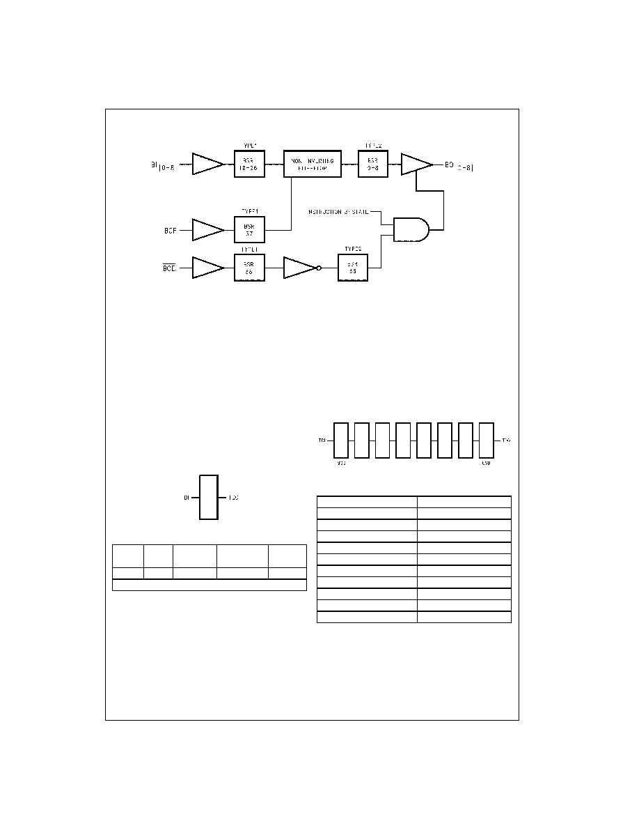
Block Diagrams (Continued)
Byte-B
Note: BSR stands for BOUNDARY-SCAN Register
Description of BOUNDARY-SCAN Circuitry
The scan cells used in the BOUNDARY-SCAN register are
one of the following two types depending upon their loca-
tion. Scan cell TYPE1 is intended to solely observe system
data, while TYPE2 has the additional ability to control sys-
tem data.
Scan cell TYPE1 is located on each system input pin while
scan cell TYPE2 is located at each system output pin as
well as at each of the two internal active-high output enable
signals. AOE controls the activity of the A-outputs while
BOE controls the activity of the B-outputs. Each will acti-
vate their respective outputs by loading a logic high.
The BYPASS register is a single bit shift register stage
identical to scan cell TYPE1. It captures a fixed logic low.
Bypass Register Scan Chain Definition
Logic 0
SCAN182374A Product IDCODE
(32-Bit Code per IEEE 1149.1)
The INSTRUCTION register is an 8-bit register which cap-
tures the default value of 10000001 (SAMPLE/PRELOAD)
during the CAPTURE-IR instruction command. The benefit
of capturing SAMPLE/PRELOAD as the default instruction
during CAPTURE-IR is that the user is no longer required
to shift in the 8-bit instruction for SAMPLE/PRELOAD. The
sequence of: CAPTURE-IR
→ EXIT1-IR → UPDATE-IR
will update the SAMPLE/PRELOAD instruction. For more
information refer to the section on instruction definitions.
Instruction Register Scan Chain Definition
Version
Entity
Per
Manufacturer Required
Number
ID
by 1149.1
0000
111111 0000000111 00000001111
1
MSB
LSB
MSB
→ LSB
Instruction Code
Instruction
00000000
EXTEST
10000001
SAMPLE/PRELOAD
10000010
CLAMP
00000011
HIGH-Z
01000001
SAMPLE-IN
01000010
SAMPLE-OUT
00100010
EXTEST-OUT
10101010
IDCODE
11111111
BYPASS
All Other
BYPASS
相关PDF资料 |
PDF描述 |
|---|---|
| SCAN182374ASSCX | |
| SCAN18374TSSCX | |
| SCANPSC100FSCX | |
| SCANPSC110FSCX | |
| SCBA15FF | 5 A, SILICON, BRIDGE RECTIFIER DIODE |
相关代理商/技术参数 |
参数描述 |
|---|---|
| SCAN182374ASSCX | 功能描述:触发器 D-Type Flip-Flop RoHS:否 制造商:Texas Instruments 电路数量:2 逻辑系列:SN74 逻辑类型:D-Type Flip-Flop 极性:Inverting, Non-Inverting 输入类型:CMOS 输出类型: 传播延迟时间:4.4 ns 高电平输出电流:- 16 mA 低电平输出电流:16 mA 电源电压-最大:5.5 V 最大工作温度:+ 85 C 安装风格:SMD/SMT 封装 / 箱体:X2SON-8 封装:Reel |
| SCAN18245/M WAF | 制造商:Texas Instruments 功能描述: |
| SCAN18245T | 制造商:NSC 制造商全称:National Semiconductor 功能描述:Non-Inverting Transceiver with TRI-STATE Outputs |
| SCAN18245TSSC | 功能描述:总线收发器 Non-Inverting Trans RoHS:否 制造商:Fairchild Semiconductor 逻辑类型:CMOS 逻辑系列:74VCX 每芯片的通道数量:16 输入电平:CMOS 输出电平:CMOS 输出类型:3-State 高电平输出电流:- 24 mA 低电平输出电流:24 mA 传播延迟时间:6.2 ns 电源电压-最大:2.7 V, 3.6 V 电源电压-最小:1.65 V, 2.3 V 最大工作温度:+ 85 C 封装 / 箱体:TSSOP-48 封装:Reel |
| SCAN18245TSSCX | 功能描述:总线收发器 Non-Inverting Trans RoHS:否 制造商:Fairchild Semiconductor 逻辑类型:CMOS 逻辑系列:74VCX 每芯片的通道数量:16 输入电平:CMOS 输出电平:CMOS 输出类型:3-State 高电平输出电流:- 24 mA 低电平输出电流:24 mA 传播延迟时间:6.2 ns 电源电压-最大:2.7 V, 3.6 V 电源电压-最小:1.65 V, 2.3 V 最大工作温度:+ 85 C 封装 / 箱体:TSSOP-48 封装:Reel |
发布紧急采购,3分钟左右您将得到回复。