参数资料
| 型号: | SE5230DR2G |
| 厂商: | ON Semiconductor |
| 文件页数: | 15/18页 |
| 文件大小: | 0K |
| 描述: | IC OP AMP LOW VOLTAGE 8-SOIC |
| 标准包装: | 2,500 |
| 放大器类型: | 通用 |
| 电路数: | 1 |
| 输出类型: | 满摆幅 |
| 转换速率: | 0.25 V/µs |
| 增益带宽积: | 600kHz |
| 电流 - 输入偏压: | 40nA |
| 电压 - 输入偏移: | 400µV |
| 电流 - 电源: | 1.1mA |
| 电流 - 输出 / 通道: | 32mA |
| 电压 - 电源,单路/双路(±): | 1.8 V ~ 15 V,±0.9 V ~ 7.5 V |
| 工作温度: | -40°C ~ 125°C |
| 安装类型: | 表面贴装 |
| 封装/外壳: | 8-SOIC(0.154",3.90mm 宽) |
| 供应商设备封装: | 8-SOICN |
| 包装: | 带卷 (TR) |
NE5230, SA5230, SE5230
http://onsemi.com
6
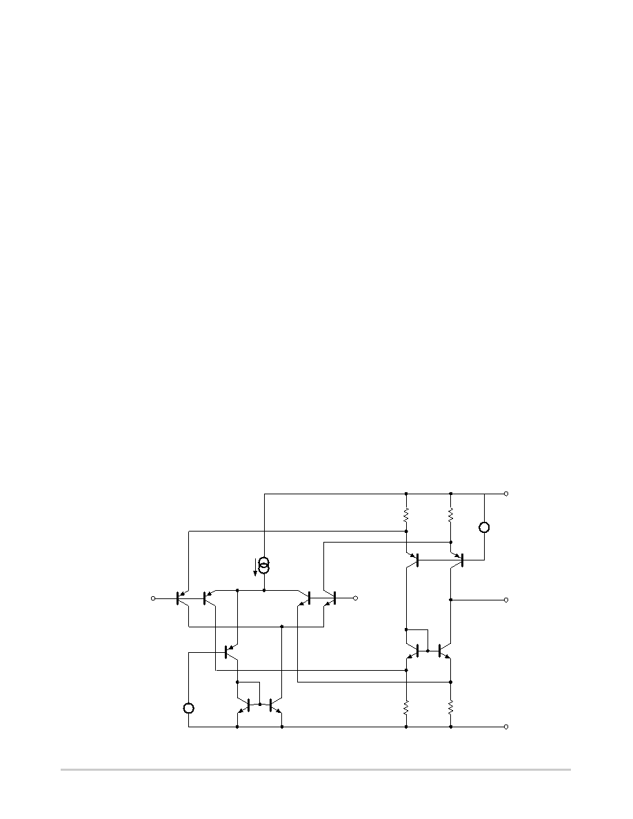
THEORY OF OPERATION
Input Stage
Operational amplifiers which are able to function at
minimum supply voltages should have input and output
stage swings capable of reaching both supply voltages
within a few millivolts in order to achieve ease of quiescent
biasing and to have maximum input/output signal handling
capability. The input stage of the NE5230 has a
commonmode voltage range that not only includes the
entire supply voltage range, but also allows either supply to
be exceeded by 250 mV without increasing the input offset
voltage by more than 6.0 mV. This is unequalled by any
other operational amplifier today.
In order to accomplish the feat of railtorail input
commonmode range, two emittercoupled differential
pairs are placed in parallel so that the commonmode
voltage of one can reach the positive supply rail and the other
can reach the negative supply rail. The simplified schematic
of Figure 1 shows how the complementary emittercoupler
transistors are configured to form the basic input stage cell.
Commonmode input signal voltages in the range from
0.8 V above VEE to VCC are handled completely by the NPN
pair, Q3 and Q4, while commonmode input signal voltages
in the range of VEE to 0.8 V above VEE are processed only
by the PNP pair, Q1 and Q2. The intermediate range of input
voltages requires that both the NPN and PNP pairs are
operating. The collector currents of the input transistors are
summed by the current combiner circuit composed of
transistors Q8 through Q11 into one output current.
Transistor Q8 is connected as a diode to ensure that the
outputs of Q2 and Q4 are properly subtracted from those of
Q1 and Q3.
The input stage was designed to overcome two important
problems for railtorail capability. As the commonmode
voltage moves from the range where only the NPN pair was
operating to where both of the input pairs were operating, the
effective transconductance would change by a factor of two.
Frequency compensation for the ranges where one input pair
was operating would, of course, not be optimal for the range
where both pairs were operating. Secondly, fast changes in
the commonmode voltage would abruptly saturate and
restore the emitter current sources, causing transient
distortion. These problems were overcome by assuring that
only the input transistor pair which is able to function
properly is active. The NPN pair is normally activated by the
current source IB1 through Q5 and the current mirror Q6 and
Q7, assuming the PNP pair is nonconducting. When the
commonmode input voltage passes below the reference
voltage, VB1 0.8 V at the base of Q5, the emitter current is
gradually steered toward the PNP pair, away from the NPN
pair. The transfer of the emitter currents between the
complementary input pairs occurs in a voltage range of
about 120 mV around the reference voltage VB1. In this way
the sum of the emitter currents for each of the NPN and PNP
transistor pairs is kept constant; this ensures that the
transconductance of the parallel combination will be
constant, since the transconductance of bipolar transistors is
proportional to their emitter currents.
An essential requirement of this kind of input stage is to
minimize the changes in input offset voltage between that of
the NPN and PNP transistor pair which occurs when the
input commonmode voltage crosses the internal reference
voltage, VB1. Careful circuit layout with a crosscoupled
quad for each input pair has yielded a typical input offset
voltage of less than 0.3 mV and a change in the input offset
voltage of less than 0.1 mV.
V
R10
R11
R8
R9
Q3
Q1
Q2
Q4
Q10
Q11
Q5
Q6
Q7
Q8
Q9
VEE
VCC
IOUT
Vb2
+
+V
b1
VIN
VIN+
Ib1
Figure 1. Input Stage
相关PDF资料 |
PDF描述 |
|---|---|
| P6SMB9.1AT3G | TVS ZENER UNIDIR 600W 9.1V SMB |
| CRCW04021R96FKED | RES 1.96 OHM 1/16W 1% 0402 SMD |
| CRM2512-FX-R300ELF | RES .300 OHM 2W 1% 2512 SMD |
| P6SMB8.2AT3G | TVS ZENER UNIDIR 600W 8.2V SMB |
| ISL28117FUZ-T7 | IC OPAMP GP 1.5MHZ LP 8MSOP |
相关代理商/技术参数 |
参数描述 |
|---|---|
| SE5234N,112 | 功能描述:运算放大器 - 运放 MATCHED QUAD HI-PER OPAMP40-85 RoHS:否 制造商:STMicroelectronics 通道数量:4 共模抑制比(最小值):63 dB 输入补偿电压:1 mV 输入偏流(最大值):10 pA 工作电源电压:2.7 V to 5.5 V 安装风格:SMD/SMT 封装 / 箱体:QFN-16 转换速度:0.89 V/us 关闭:No 输出电流:55 mA 最大工作温度:+ 125 C 封装:Reel |
| SE5234N/01,112 | 功能描述:IC OPAMP MATCHED QUAD HP 14-DIP RoHS:是 类别:集成电路 (IC) >> Linear - Amplifiers - Instrumentation 系列:- 标准包装:1,000 系列:- 放大器类型:电压反馈 电路数:4 输出类型:满摆幅 转换速率:33 V/µs 增益带宽积:20MHz -3db带宽:30MHz 电流 - 输入偏压:2nA 电压 - 输入偏移:3000µV 电流 - 电源:2.5mA 电流 - 输出 / 通道:30mA 电压 - 电源,单路/双路(±):4.5 V ~ 16.5 V,±2.25 V ~ 8.25 V 工作温度:-40°C ~ 85°C 安装类型:表面贴装 封装/外壳:14-SOIC(0.154",3.90mm 宽) 供应商设备封装:14-SOIC 包装:带卷 (TR) |
| SE529H | 制造商:SNT 功能描述: |
| SE529K | 制造商:Texas Instruments 功能描述:IC COMPARATOR HS DIFF TO100-10 制造商:Texas Instruments 功能描述:High Speed Differential Comparator |
| SE5300-614 | 制造商: 功能描述: 制造商:ROBERTSHAW CONTROLS CO 功能描述: 制造商:undefined 功能描述: |
发布紧急采购,3分钟左右您将得到回复。