参数资料
| 型号: | SE5230DR2G |
| 厂商: | ON Semiconductor |
| 文件页数: | 16/18页 |
| 文件大小: | 0K |
| 描述: | IC OP AMP LOW VOLTAGE 8-SOIC |
| 标准包装: | 2,500 |
| 放大器类型: | 通用 |
| 电路数: | 1 |
| 输出类型: | 满摆幅 |
| 转换速率: | 0.25 V/µs |
| 增益带宽积: | 600kHz |
| 电流 - 输入偏压: | 40nA |
| 电压 - 输入偏移: | 400µV |
| 电流 - 电源: | 1.1mA |
| 电流 - 输出 / 通道: | 32mA |
| 电压 - 电源,单路/双路(±): | 1.8 V ~ 15 V,±0.9 V ~ 7.5 V |
| 工作温度: | -40°C ~ 125°C |
| 安装类型: | 表面贴装 |
| 封装/外壳: | 8-SOIC(0.154",3.90mm 宽) |
| 供应商设备封装: | 8-SOICN |
| 包装: | 带卷 (TR) |
NE5230, SA5230, SE5230
http://onsemi.com
7
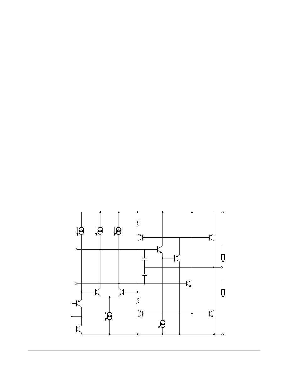
Output Stage
Processing output voltage swings that nominally reach to
less than 100 mV of either supply voltage can only be
achieved by a pair of complementary commonemitter
connected transistors. Normally, such a configuration
causes complex feedforward signal paths that develop by
combining biasing and driving which can be found in
previous low supply voltage designs. The unique output
stage of the NE5230 separates the functions of driving and
biasing, as shown in the simplified schematic of Figure 2 and
has the advantage of a shorter signal path which leads to
increasing the effective bandwidth.
This output stage consists of two parts: the Darlington
output transistors and the class AB control regulator. The
output transistor Q3 connected with the Darlington
transistors Q4 and Q5 can source up to 10 mA to an output
load. The output of NPN Darlington connected transistors
Q1 and Q2 together are able to sink an output current of
10 mA. Accurate and efficient class AB control is necessary
to insure that none of the output transistors are ever
completely cut off. This is accomplished by the differential
amplifier (formed by Q8 and Q9) which controls the biasing
of the output transistors. The differential amplifier compares
the summed voltages across two diodes, D1 and D2, at the
base of Q8 with the summed voltages across the
baseemitter diodes of the output transistors Q1 and Q3. The
baseemitter voltage of Q3 is converted into a current by Q6
and R6 and reconverted into a voltage across the
baseemitter diode of Q7 and R7. The summed voltage
across the baseemitter diodes of the output transistors Q3
and Q1 is proportional to the logarithm of the product of the
push and pull currents IOP and ION, respectively. The
combined voltages across diodes D1 and D2 are
proportional to the logarithm of the square of the reference
current IB1. When the diode characteristics and
temperatures of the pairs Q1, D1 and Q3, Q2 are equal, the
relation IOP × ION IB1 × IB1 is satisfied.
Separating the functions of biasing and driving prevents
the driving signals from becoming delayed by the biasing
circuit. The output Darlington transistors are directly
accessible for inphase driving signals on the bases of Q5
and Q2. This is very important for simple highfrequency
compensation. The output transistors can be highfrequency
compensated by Miller capacitors CM1A and CM1B
connected from the collectors to the bases of the output
Darlington transistors.
A generalpurpose op amp of this type must have enough
openloop gain for applications when the output is driving
a low resistance load. The NE5230 accomplishes this by
inserting an intermediate commonemitter stage between
the input and output stages. The three stages provide a very
large gain, but the op amp now has three natural dominant
poles one at the output of each commonemitter stage.
Frequency compensation is implemented with a simple
scheme of nested, polesplitting Miller integrators. The
Miller capacitors CM1A and CM1B are the first part of the
nested structure, and provide compensation for the output
and intermediate stages. A second pair of Miller integrators
provide polesplitting compensation for the pole from the
input stage and the pole resulting from the compensated
combination of poles from the intermediate and output
stages. The result is a stable, internallycompensated op
amp with a phase margin of 70
°.
Q5
Ib1
Ib2
Ib3
Ib5
Ib4
Q4
Q6
Q8
Q9
D1
Q7
Q3
D2
Q1
Q2
R7
R6
CM1B
CM1A
Vb2
Vb5
VCC
VEE
VOUT
IOP
ION
Figure 2. Output Stage
相关PDF资料 |
PDF描述 |
|---|---|
| P6SMB9.1AT3G | TVS ZENER UNIDIR 600W 9.1V SMB |
| CRCW04021R96FKED | RES 1.96 OHM 1/16W 1% 0402 SMD |
| CRM2512-FX-R300ELF | RES .300 OHM 2W 1% 2512 SMD |
| P6SMB8.2AT3G | TVS ZENER UNIDIR 600W 8.2V SMB |
| ISL28117FUZ-T7 | IC OPAMP GP 1.5MHZ LP 8MSOP |
相关代理商/技术参数 |
参数描述 |
|---|---|
| SE5234N,112 | 功能描述:运算放大器 - 运放 MATCHED QUAD HI-PER OPAMP40-85 RoHS:否 制造商:STMicroelectronics 通道数量:4 共模抑制比(最小值):63 dB 输入补偿电压:1 mV 输入偏流(最大值):10 pA 工作电源电压:2.7 V to 5.5 V 安装风格:SMD/SMT 封装 / 箱体:QFN-16 转换速度:0.89 V/us 关闭:No 输出电流:55 mA 最大工作温度:+ 125 C 封装:Reel |
| SE5234N/01,112 | 功能描述:IC OPAMP MATCHED QUAD HP 14-DIP RoHS:是 类别:集成电路 (IC) >> Linear - Amplifiers - Instrumentation 系列:- 标准包装:1,000 系列:- 放大器类型:电压反馈 电路数:4 输出类型:满摆幅 转换速率:33 V/µs 增益带宽积:20MHz -3db带宽:30MHz 电流 - 输入偏压:2nA 电压 - 输入偏移:3000µV 电流 - 电源:2.5mA 电流 - 输出 / 通道:30mA 电压 - 电源,单路/双路(±):4.5 V ~ 16.5 V,±2.25 V ~ 8.25 V 工作温度:-40°C ~ 85°C 安装类型:表面贴装 封装/外壳:14-SOIC(0.154",3.90mm 宽) 供应商设备封装:14-SOIC 包装:带卷 (TR) |
| SE529H | 制造商:SNT 功能描述: |
| SE529K | 制造商:Texas Instruments 功能描述:IC COMPARATOR HS DIFF TO100-10 制造商:Texas Instruments 功能描述:High Speed Differential Comparator |
| SE5300-614 | 制造商: 功能描述: 制造商:ROBERTSHAW CONTROLS CO 功能描述: 制造商:undefined 功能描述: |
发布紧急采购,3分钟左右您将得到回复。