- 您现在的位置:买卖IC网 > PDF目录10988 > SI3216M-B-GM (Silicon Laboratories Inc)IC SLIC/CODEC 1CH 38QFN PDF资料下载
参数资料
| 型号: | SI3216M-B-GM |
| 厂商: | Silicon Laboratories Inc |
| 文件页数: | 50/122页 |
| 文件大小: | 0K |
| 描述: | IC SLIC/CODEC 1CH 38QFN |
| 标准包装: | 43 |
| 系列: | ProSLIC® |
| 功能: | 用户线路接口概念(SLIC),CODEC |
| 接口: | GCI,PCM,SPI |
| 电路数: | 1 |
| 电源电压: | 3.13 V ~ 5.25 V |
| 电流 - 电源: | 88mA |
| 功率(瓦特): | 700mW |
| 工作温度: | -40°C ~ 85°C |
| 安装类型: | 表面贴装 |
| 封装/外壳: | 38-VFQFN 裸露焊盘 |
| 供应商设备封装: | 38-QFN(5x7) |
| 包装: | 管件 |
| 包括: | 音频音调生成,BORSCHT 功能,FSK 生成,振铃和电池电压生成 |
第1页第2页第3页第4页第5页第6页第7页第8页第9页第10页第11页第12页第13页第14页第15页第16页第17页第18页第19页第20页第21页第22页第23页第24页第25页第26页第27页第28页第29页第30页第31页第32页第33页第34页第35页第36页第37页第38页第39页第40页第41页第42页第43页第44页第45页第46页第47页第48页第49页当前第50页第51页第52页第53页第54页第55页第56页第57页第58页第59页第60页第61页第62页第63页第64页第65页第66页第67页第68页第69页第70页第71页第72页第73页第74页第75页第76页第77页第78页第79页第80页第81页第82页第83页第84页第85页第86页第87页第88页第89页第90页第91页第92页第93页第94页第95页第96页第97页第98页第99页第100页第101页第102页第103页第104页第105页第106页第107页第108页第109页第110页第111页第112页第113页第114页第115页第116页第117页第118页第119页第120页第121页第122页
Si3216
Rev. 1.0
33
Not
Recommended
fo
r N
ew
D
esi
gn
s
2.1.9. Linefeed Calibration
An internal calibration algorithm corrects for internal and
external component errors. The calibration is initiated by
setting the CAL bit in direct Register 96. Upon
completion
of
the
calibration
cycle,
this
bit
is
automatically reset.
It is recommended that a calibration be executed
following system powerup. Upon release of the chip
reset, the ProSLIC is in the Open state. After powering
up the dc-dc converter and allowing it to settle for time
(TSETTLE) the calibration can be initiated. Additional
calibrations may be performed, but only one calibration
should be necessary as long as the system remains
powered up.
During calibration, VBAT, VTIP, and VRING voltages are
controlled by the calibration engine to provide the
correct external voltage conditions for the algorithm.
Calibration should be performed in the On-Hook state.
RING or TIP must not be connected to ground during
the calibration.
When using the Si3201, automatic calibration routines
for RING gain mismatch and TIP gain mismatch should
not be performed. Instead of running these two
calibrations automatically, consult “AN35: Si321x User’s
Quick Reference Guide”, and follow the instructions for
manual calibration.
2.2. Battery Voltage Generation and
Switching
The ProSLIC integrates a dc-dc converter controller that
dynamically regulates a single output voltage. This
mode eliminates the need to supply large external
battery voltages. Instead, it converts a single positive
input voltage into the real-time battery voltage needed
for any given state according to programmed linefeed
parameters.
2.2.1. DC-DC Converter General Description
The dc-dc converter dynamically generates the large
negative voltages required to operate the linefeed
interface. The ProSLIC acts as the controller for a buck-
boost dc-dc converter that converts a positive dc
voltage into the desired negative battery voltage. In
addition to eliminating external power supplies, this
allows the ProSLIC to dynamically control the battery
voltage to the minimum required for any given mode of
operation.
Two different dc-dc circuit options are offered: a BJT/
inductor version and a MOSFET/transformer version.
Due to the differences on the driving circuits, there are
two different versions of the ProSLIC. The Si321x
supports the BJT/inductor circuit option, and the
Si321xM version supports the MOSFET solution. The
only difference between the two versions is the polarity
of the DCFF pin with respect to the DCDRV pin. For the
Si321x, DCDRV and DCFF are opposite polarity. For
the Si321xM, DCDRV and DCFF are the same polarity.
Table 26 summarizes these differences.
Extensive design guidance on each of these circuits can
be obtained from “AN45: Design Guide for the Si3210
DC-DC Converter” and from an interactive dc-dc
converter design spreadsheet. Both of these documents
are available on the Silicon Laboratories website
(www.silabs.com).
2.2.2. BJT/Inductor Circuit Option Using Si321x
The BJT/Inductor circuit option, as defined in Figure 13
on page 23, offers a flexible, low-cost solution.
Depending on selected L1 inductance value and the
switching frequency, the input voltage (VDC) can range
from 5 V to 30 V. By nature of a dc-dc converter’s
operation, peak and average input currents can become
large with small input voltages. Consider this when
selecting the appropriate input voltage and power rating
for the VDC power supply.
For this solution, a PNP power BJT (Q7) switches the
current flow through low ESR inductor L1. The Si3216
uses the DCDRV and DCFF pins to switch Q7 on and
off. DCDRV controls Q7 through NPN BJT Q8. DCFF is
ac-coupled to Q7 through capacitor C10 to assist R16 in
turning off Q7. Therefore, DCFF must have opposite
polarity to DCDRV, and the Si321x (not Si321xM) must
be used.
2.2.3. MOSFET/Transformer Circuit Option Using
Si321xM
The MOSFET/transformer circuit option, as defined in
Figure 14 on page 24, offers higher power efficiencies
across a larger input voltage range. Depending on the
transformer’s primary inductor value and the switching
frequency, the input voltage (VDC) can range from 3.3 V
to 35 V. Therefore, it is possible to power the entire
ProSLIC solution from a single 3.3 V or 5 V power
supply. By nature of a dc-dc converter’s operation, peak
and average input currents can become large with small
input voltages. Consider this when selecting the
appropriate input voltage and power rating for the VDC
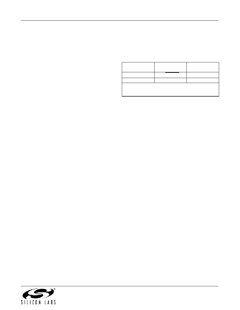
Table 26. Si321x and Si321xM Differences
Device
DCFF Signal
Polarity
DCPOL
Si321x
= DCDRV
0
Si321xM
= DCDRV
1
Notes:
1. DCFF signal polarity with respect to DCDRV signal.
2. Direct Register 93, bit 5; This is a read-only bit.
相关PDF资料 |
PDF描述 |
|---|---|
| SI3216M-B-FM | IC SLIC/CODEC 1CH 38QFN |
| VI-B0N-IY-F2 | CONVERTER MOD DC/DC 18.5V 50W |
| VI-B0N-IY-F1 | CONVERTER MOD DC/DC 18.5V 50W |
| VI-B0L-IY-F4 | CONVERTER MOD DC/DC 28V 50W |
| VI-B0L-IY-F2 | CONVERTER MOD DC/DC 28V 50W |
相关代理商/技术参数 |
参数描述 |
|---|---|
| SI3216M-BT | 功能描述:IC SLIC/CODEC 1CH 38TSSOP RoHS:否 类别:集成电路 (IC) >> 接口 - 电信 系列:ProSLIC® 产品培训模块:Lead (SnPb) Finish for COTS 产品变化通告:Product Discontinuation 06/Feb/2012 标准包装:750 系列:* |
| SI3216M-C-FM | 功能描述:电信线路管理 IC Single-Channel Wide- band SLIC/Codec RoHS:否 制造商:STMicroelectronics 产品:PHY 接口类型:UART 电源电压-最大:18 V 电源电压-最小:8 V 电源电流:30 mA 最大工作温度:+ 85 C 最小工作温度:- 40 C 安装风格:SMD/SMT 封装 / 箱体:VFQFPN-48 封装:Tray |
| SI3216M-C-FMR | 功能描述:电信线路管理 IC SnglCH WB SLIC/Codec Transformer dc-dc RoHS:否 制造商:STMicroelectronics 产品:PHY 接口类型:UART 电源电压-最大:18 V 电源电压-最小:8 V 电源电流:30 mA 最大工作温度:+ 85 C 最小工作温度:- 40 C 安装风格:SMD/SMT 封装 / 箱体:VFQFPN-48 封装:Tray |
| SI3216M-C-GM | 功能描述:电信线路管理 IC Single-Channel Wide- band SLIC/Codec RoHS:否 制造商:STMicroelectronics 产品:PHY 接口类型:UART 电源电压-最大:18 V 电源电压-最小:8 V 电源电流:30 mA 最大工作温度:+ 85 C 最小工作温度:- 40 C 安装风格:SMD/SMT 封装 / 箱体:VFQFPN-48 封装:Tray |
| SI3216M-C-GMR | 功能描述:电信线路管理 IC SnglCH WB SLIC/Codec Transformer dc-dc RoHS:否 制造商:STMicroelectronics 产品:PHY 接口类型:UART 电源电压-最大:18 V 电源电压-最小:8 V 电源电流:30 mA 最大工作温度:+ 85 C 最小工作温度:- 40 C 安装风格:SMD/SMT 封装 / 箱体:VFQFPN-48 封装:Tray |
发布紧急采购,3分钟左右您将得到回复。