- 您现在的位置:买卖IC网 > PDF目录10988 > SI3216M-B-GM (Silicon Laboratories Inc)IC SLIC/CODEC 1CH 38QFN PDF资料下载
参数资料
| 型号: | SI3216M-B-GM |
| 厂商: | Silicon Laboratories Inc |
| 文件页数: | 64/122页 |
| 文件大小: | 0K |
| 描述: | IC SLIC/CODEC 1CH 38QFN |
| 标准包装: | 43 |
| 系列: | ProSLIC® |
| 功能: | 用户线路接口概念(SLIC),CODEC |
| 接口: | GCI,PCM,SPI |
| 电路数: | 1 |
| 电源电压: | 3.13 V ~ 5.25 V |
| 电流 - 电源: | 88mA |
| 功率(瓦特): | 700mW |
| 工作温度: | -40°C ~ 85°C |
| 安装类型: | 表面贴装 |
| 封装/外壳: | 38-VFQFN 裸露焊盘 |
| 供应商设备封装: | 38-QFN(5x7) |
| 包装: | 管件 |
| 包括: | 音频音调生成,BORSCHT 功能,FSK 生成,振铃和电池电压生成 |
第1页第2页第3页第4页第5页第6页第7页第8页第9页第10页第11页第12页第13页第14页第15页第16页第17页第18页第19页第20页第21页第22页第23页第24页第25页第26页第27页第28页第29页第30页第31页第32页第33页第34页第35页第36页第37页第38页第39页第40页第41页第42页第43页第44页第45页第46页第47页第48页第49页第50页第51页第52页第53页第54页第55页第56页第57页第58页第59页第60页第61页第62页第63页当前第64页第65页第66页第67页第68页第69页第70页第71页第72页第73页第74页第75页第76页第77页第78页第79页第80页第81页第82页第83页第84页第85页第86页第87页第88页第89页第90页第91页第92页第93页第94页第95页第96页第97页第98页第99页第100页第101页第102页第103页第104页第105页第106页第107页第108页第109页第110页第111页第112页第113页第114页第115页第116页第117页第118页第119页第120页第121页第122页
Si3216
46
Rev. 1.0
Not
Recommended
fo
r N
ew
D
esi
gn
s
subscriber loop via the ITIPP and IRINGP pins through
an off-chip current buffer (IBUF), which is implemented
using transistors Q1 and Q2 (see Figure on page 22).
Gm is referenced to an off-chip resistor (R15).
The ProSLIC also provides a means of compensating
for degraded subscriber loop conditions involving
excessive line capacitance (leakage). The CLC[1:0] bits
of direct Register 10 increase the ac signal magnitude
to compensate for the additional loss at the high end of
the audio frequency range. The default setting of
CLC[2:0] assumes no line capacitance.
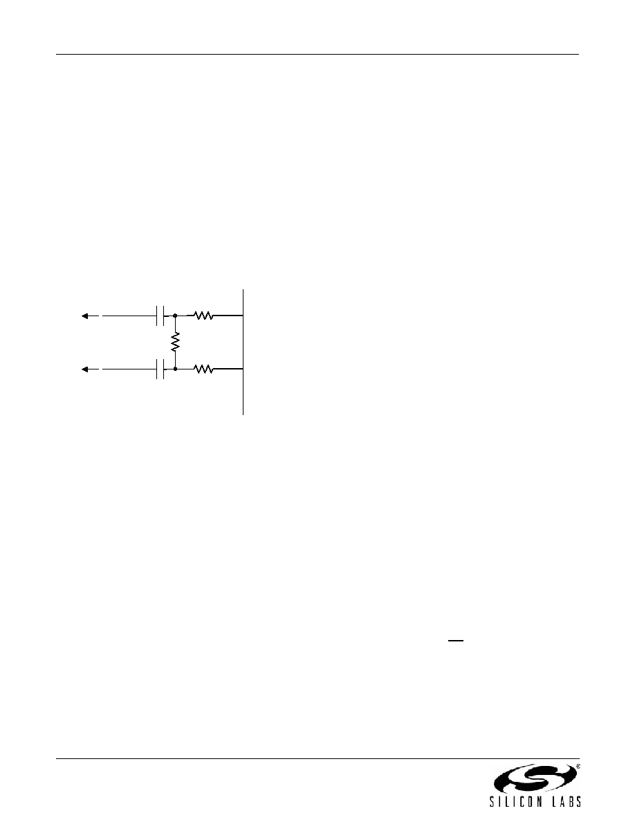
When 600 + 1 F or 900 + 2.16 F impedances are
selected, an internal reference resistor is removed from
the impedance synthesis circuit to accommodate an
external resistor, RZREF, inserted into the application
circuit as shown in Figure 25.
Figure 25. RZREF External Resistor Placement
2.7. Clock Generation
The ProSLIC generates the necessary internal clock
frequencies from the PCLK input. PCLK must be
synchronous to the 8 kHz FSYNC clock and run at one
of the following rates: 256kHz, 512kHz, 768kHz,
1.024 MHz, 1.536 MHz, 2.048 MHz, 4.096 MHz, or
8.192 MHz. The ratio of the PCLK rate to the FSYNC
rate is determined via a counter clocked by PCLK. The
three-bit ratio information is automatically transferred
into an internal register, PLL_MULT, following a reset of
the ProSLIC. The internal PLL_MULT register is used to
control the internal PLL, which multiplies PCLK as
needed to generate the 16.384 MHz rate needed to run
the internal filters and other circuitry.
The PLL clock synthesizer settles very quickly following
powerup. However, the settling time depends on the
PCLK frequency and it can be approximately predicted
by the following equation:
2.8. Interrupt Logic
The ProSLIC is capable of generating interrupts for the
following events:
Loop current/ring ground detected
Ring trip detected
Power alarm
Active timer 1 expired
Inactive timer 1 expired
Active timer 2 expired
Inactive timer 2 expired
Ringing active timer expired
Ringing inactive timer expired
Indirect register access complete
The interface to the interrupt logic consists of six
registers. Three interrupt status registers contain 1 bit
for each of the above interrupt functions. These bits are
set when an interrupt is pending for the associated
resource. Three interrupt enable registers also contain 1
bit for each interrupt function. In the case of the interrupt
enable registers, the bits are active high. Refer to the
appropriate
functional
description
section
for
operational details of the interrupt functions.
When a resource reaches an interrupt condition, it
signals an interrupt to the interrupt control block. The
interrupt control block then sets the associated bit in the
interrupt status register if the enable bit for that interrupt
is set. The INT pin is an open-drain output and a NOR
of the bits of the interrupt status registers. Therefore, if a
bit in the interrupt status registers is asserted, IRQ
asserts low. Upon receiving the interrupt, the interrupt
handler should read interrupt status registers to
determine which resource is requesting service. To
clear a pending interrupt, write the desired bit in the
appropriate interrupt status register to 1. Writing a 0 has
no effect. This provides a mechanism for clearing
individual
bits
when
multiple
interrupts
occur
simultaneously. While the interrupt status registers are
non-zero, the INT pin will remain asserted.
2.9. Serial Peripheral Interface
The control interface to the ProSLIC is a 4-wire interface
modeled after commonly-available microcontroller and
serial peripheral devices. The interface consists of a
clock (SCLK), chip select (CS), serial data input (SDI),
and serial data output (SDO). Data is transferred a byte
at a time with each register access consisting of a pair
write operation in the SPI bus.
The first byte of the pair is the command/address byte.
The MSB of this byte indicates a register read when 1
and a register write when 0. The remaining seven bits of
to TIP
to RING
Si3216
STIPAC
SRINGAC
R
ZREF
C3
C4
R8
R9
For 600 + 1
F, R
ZREF = 12 k and C3, C4 = 100 nF
For 900 + 2.16
F, R
ZREF = 18 k and C3, C4 = 220 nF
T
SETTLE
64
F
PCLK
-----------------
=
相关PDF资料 |
PDF描述 |
|---|---|
| SI3216M-B-FM | IC SLIC/CODEC 1CH 38QFN |
| VI-B0N-IY-F2 | CONVERTER MOD DC/DC 18.5V 50W |
| VI-B0N-IY-F1 | CONVERTER MOD DC/DC 18.5V 50W |
| VI-B0L-IY-F4 | CONVERTER MOD DC/DC 28V 50W |
| VI-B0L-IY-F2 | CONVERTER MOD DC/DC 28V 50W |
相关代理商/技术参数 |
参数描述 |
|---|---|
| SI3216M-BT | 功能描述:IC SLIC/CODEC 1CH 38TSSOP RoHS:否 类别:集成电路 (IC) >> 接口 - 电信 系列:ProSLIC® 产品培训模块:Lead (SnPb) Finish for COTS 产品变化通告:Product Discontinuation 06/Feb/2012 标准包装:750 系列:* |
| SI3216M-C-FM | 功能描述:电信线路管理 IC Single-Channel Wide- band SLIC/Codec RoHS:否 制造商:STMicroelectronics 产品:PHY 接口类型:UART 电源电压-最大:18 V 电源电压-最小:8 V 电源电流:30 mA 最大工作温度:+ 85 C 最小工作温度:- 40 C 安装风格:SMD/SMT 封装 / 箱体:VFQFPN-48 封装:Tray |
| SI3216M-C-FMR | 功能描述:电信线路管理 IC SnglCH WB SLIC/Codec Transformer dc-dc RoHS:否 制造商:STMicroelectronics 产品:PHY 接口类型:UART 电源电压-最大:18 V 电源电压-最小:8 V 电源电流:30 mA 最大工作温度:+ 85 C 最小工作温度:- 40 C 安装风格:SMD/SMT 封装 / 箱体:VFQFPN-48 封装:Tray |
| SI3216M-C-GM | 功能描述:电信线路管理 IC Single-Channel Wide- band SLIC/Codec RoHS:否 制造商:STMicroelectronics 产品:PHY 接口类型:UART 电源电压-最大:18 V 电源电压-最小:8 V 电源电流:30 mA 最大工作温度:+ 85 C 最小工作温度:- 40 C 安装风格:SMD/SMT 封装 / 箱体:VFQFPN-48 封装:Tray |
| SI3216M-C-GMR | 功能描述:电信线路管理 IC SnglCH WB SLIC/Codec Transformer dc-dc RoHS:否 制造商:STMicroelectronics 产品:PHY 接口类型:UART 电源电压-最大:18 V 电源电压-最小:8 V 电源电流:30 mA 最大工作温度:+ 85 C 最小工作温度:- 40 C 安装风格:SMD/SMT 封装 / 箱体:VFQFPN-48 封装:Tray |
发布紧急采购,3分钟左右您将得到回复。