- 您现在的位置:买卖IC网 > PDF目录18553 > SI3445DV-T1-E3 (Vishay Siliconix)MOSFET P-CH 8V 6-TSOP PDF资料下载
参数资料
| 型号: | SI3445DV-T1-E3 |
| 厂商: | Vishay Siliconix |
| 文件页数: | 6/9页 |
| 文件大小: | 0K |
| 描述: | MOSFET P-CH 8V 6-TSOP |
| 标准包装: | 3,000 |
| 系列: | TrenchFET® |
| FET 型: | MOSFET P 通道,金属氧化物 |
| FET 特点: | 逻辑电平门 |
| 漏极至源极电压(Vdss): | 8V |
| 开态Rds(最大)@ Id, Vgs @ 25° C: | 42 毫欧 @ 5.6A,4.5V |
| Id 时的 Vgs(th)(最大): | 1V @ 250µA |
| 闸电荷(Qg) @ Vgs: | 25nC @ 4.5V |
| 安装类型: | 表面贴装 |
| 封装/外壳: | 6-TSOP(0.065",1.65mm 宽) |
| 供应商设备封装: | 6-TSOP |
| 包装: | 带卷 (TR) |
�� �
�
�AN823�
�Vishay� Siliconix�
�Mounting� LITTLE� FOOT� R� TSOP-6� Power� MOSFETs�
�Surface� mounted� power� MOSFET� packaging� has� been� based� on�
�integrated� circuit� and� small� signal� packages.� Those� packages�
�have� been� modified� to� provide� the� improvements� in� heat� transfer�
�required� by� power� MOSFETs.� Leadframe� materials� and� design,�
�molding� compounds,� and� die� attach� materials� have� been�
�changed.� What� has� remained� the� same� is� the� footprint� of� the�
�packages.�
�The� basis� of� the� pad� design� for� surface� mounted� power� MOSFET�
�is� the� basic� footprint� for� the� package.� For� the� TSOP-6� package�
�outline� drawing� see� http://www.vishay.com/doc?71200� and� see�
�http://www.vishay.com/doc?72610� for� the� minimum� pad� footprint.�
�In� converting� the� footprint� to� the� pad� set� for� a� power� MOSFET,� you�
�must� remember� that� not� only� do� you� want� to� make� electrical�
�connection� to� the� package,� but� you� must� made� thermal� connection�
�and� provide� a� means� to� draw� heat� from� the� package,� and� move� it�
�away� from� the� package.�
�In� the� case� of� the� TSOP-6� package,� the� electrical� connections� are�
�very� simple.� Pins� 1,� 2,� 5,� and� 6� are� the� drain� of� the� MOSFET� and�
�are� connected� together.� For� a� small� signal� device� or� integrated�
�circuit,� typical� connections� would� be� made� with� traces� that� are�
�0.020� inches� wide.� Since� the� drain� pins� serve� the� additional�
�function� of� providing� the� thermal� connection� to� the� package,� this�
�level� of� connection� is� inadequate.� The� total� cross� section� of� the�
�copper� may� be� adequate� to� carry� the� current� required� for� the�
�application,� but� it� presents� a� large� thermal� impedance.� Also,� heat�
�spreads� in� a� circular� fashion� from� the� heat� source.� In� this� case� the�
�drain� pins� are� the� heat� sources� when� looking� at� heat� spread� on� the�
�PC� board.�
�Figure� 1� shows� the� copper� spreading� recommended� footprint� for�
�the� TSOP-6� package.� This� pattern� shows� the� starting� point� for�
�utilizing� the� board� area� available� for� the� heat� spreading� copper.� To�
�create� this� pattern,� a� plane� of� copper� overlays� the� basic� pattern� on�
�pins� 1,2,5,� and� 6.� The� copper� plane� connects� the� drain� pins�
�electrically,� but� more� importantly� provides� planar� copper� to� draw�
�heat� from� the� drain� leads� and� start� the� process� of� spreading� the�
�heat� so� it� can� be� dissipated� into� the� ambient� air.� Notice� that� the�
�planar� copper� is� shaped� like� a� “T”� to� move� heat� away� from� the�
�drain� leads� in� all� directions.� This� pattern� uses� all� the� available� area�
�underneath� the� body� for� this� purpose.�
�0.167�
�4.25�
�Since� surface� mounted� packages� are� small,� and� reflow� soldering�
�is� the� most� common� form� of� soldering� for� surface� mount�
�components,� “thermal”� connections� from� the� planar� copper� to� the�
�pads� have� not� been� used.� Even� if� additional� planar� copper� area� is�
�used,� there� should� be� no� problems� in� the� soldering� process.� The�
�actual� solder� connections� are� defined� by� the� solder� mask�
�openings.� By� combining� the� basic� footprint� with� the� copper� plane�
�on� the� drain� pins,� the� solder� mask� generation� occurs� automatically.�
�A� final� item� to� keep� in� mind� is� the� width� of� the� power� traces.� The�
�absolute� minimum� power� trace� width� must� be� determined� by� the�
�amount� of� current� it� has� to� carry.� For� thermal� reasons,� this�
�minimum� width� should� be� at� least� 0.020� inches.� The� use� of� wide�
�traces� connected� to� the� drain� plane� provides� a� low� impedance�
�path� for� heat� to� move� away� from� the� device.�
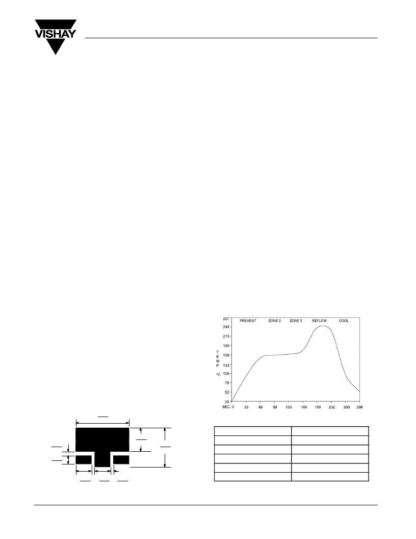
�REFLOW� SOLDERING�
�Vishay� Siliconix� surface-mount� packages� meet� solder� reflow�
�reliability� requirements.� Devices� are� subjected� to� solder� reflow� as� a�
�test� preconditioning� and� are� then� reliability-tested� using�
�temperature� cycle,� bias� humidity,� HAST,� or� pressure� pot.� The�
�solder� reflow� temperature� profile� used,� and� the� temperatures� and�
�time� duration,� are� shown� in� Figures� 2� and� 3.�
�Ramp-Up� Rate�
�+6� _� C/Second� Maximum�
�0.014�
�0.35�
�0.026�
�0.65�
�0.074�
�1.875�
�0.122�
�3.1�
�Temperature� @� 155� "� 15� _� C�
�Temperature� Above� 180� _� C�
�Maximum� Temperature�
�Time� at� Maximum� Temperature�
�120� Seconds� Maximum�
�70� ?� 180� Seconds�
�240� +5/� ?� 0� _� C�
�20� ?� 40� Seconds�
�0.049�
�1.25�
�0.049�
�1.25�
�0.010�
�0.25�
�Ramp-Down� Rate�
�+6� _� C/Second� Maximum�
�FIGURE� 1.� Recommended� Copper� Spreading� Footprint�
�Document� Number:� 71743�
�27-Feb-04�
�FIGURE� 2.� Solder� Reflow� Temperature� Profile�
�www.vishay.com�
�1�
�相关PDF资料 |
PDF描述 |
|---|---|
| ASA-38.400MHZ-L-T3 | OSC 38.400 MHZ 3.3V SMD |
| ABM11-48.000MHZ-B7G-T | CRYSTAL 48.0000 MHZ 10PF SMD |
| DLW5BTN142SQ2L | CHOKE COMMON MODE 1400 OHM 2020 |
| 940C20S33K-F | CAP FILM 0.033UF 2KVDC AXIAL |
| ABLS-19.6608MHZ-K4T | CRYSTAL 19.66080 MHZ 18PF SMD |
相关代理商/技术参数 |
参数描述 |
|---|---|
| SI3445DV-T1-E3 | 制造商:Vishay Siliconix 功能描述:MOSFET Transistor |
| SI3445DV-T1-GE3 | 功能描述:MOSFET 8.0V 5.6A 2.0W 42mohm @ 4.5V RoHS:否 制造商:STMicroelectronics 晶体管极性:N-Channel 汲极/源极击穿电压:650 V 闸/源击穿电压:25 V 漏极连续电流:130 A 电阻汲极/源极 RDS(导通):0.014 Ohms 配置:Single 最大工作温度: 安装风格:Through Hole 封装 / 箱体:Max247 封装:Tube |
| SI3446ADV | 制造商:VISHAY 制造商全称:Vishay Siliconix 功能描述:N-Channel 20-V (D-S) MOSFET |
| SI3446ADV-T1-E3 | 功能描述:MOSFET 20V 6.0A 3.2W RoHS:否 制造商:STMicroelectronics 晶体管极性:N-Channel 汲极/源极击穿电压:650 V 闸/源击穿电压:25 V 漏极连续电流:130 A 电阻汲极/源极 RDS(导通):0.014 Ohms 配置:Single 最大工作温度: 安装风格:Through Hole 封装 / 箱体:Max247 封装:Tube |
| SI3446ADV-T1-GE3 | 功能描述:MOSFET 20V 6.0A 3.2W 37mohm @ 4.5V RoHS:否 制造商:STMicroelectronics 晶体管极性:N-Channel 汲极/源极击穿电压:650 V 闸/源击穿电压:25 V 漏极连续电流:130 A 电阻汲极/源极 RDS(导通):0.014 Ohms 配置:Single 最大工作温度: 安装风格:Through Hole 封装 / 箱体:Max247 封装:Tube |
发布紧急采购,3分钟左右您将得到回复。