- 您现在的位置:买卖IC网 > PDF目录2108 > SI5317A-C-GM (Silicon Laboratories Inc)IC CLK JITTER CLEANR PROG 36QFN PDF资料下载
参数资料
| 型号: | SI5317A-C-GM |
| 厂商: | Silicon Laboratories Inc |
| 文件页数: | 31/46页 |
| 文件大小: | 0K |
| 描述: | IC CLK JITTER CLEANR PROG 36QFN |
| 应用说明: | SI5315/17 Crystal Selection AppNote |
| 特色产品: | Si5317 Jitter Cleaning Clock |
| 标准包装: | 490 |
| 系列: | DSPLL® |
| 类型: | 抖动消除器 |
| PLL: | 带旁路 |
| 输入: | 时钟,晶体 |
| 输出: | CML,CMOS,LVDS,LVPECL |
| 电路数: | 1 |
| 比率 - 输入:输出: | 1:2 |
| 差分 - 输入:输出: | 是/是 |
| 频率 - 最大: | 710MHz |
| 除法器/乘法器: | 无/无 |
| 电源电压: | 1.71 V ~ 3.63 V |
| 工作温度: | -40°C ~ 85°C |
| 安装类型: | 表面贴装 |
| 封装/外壳: | 36-VFQFN 裸露焊盘 |
| 供应商设备封装: | 36-QFN(6x6) |
| 包装: | 托盘 |
| 产品目录页面: | 628 (CN2011-ZH PDF) |
| 其它名称: | 336-1923 |
第1页第2页第3页第4页第5页第6页第7页第8页第9页第10页第11页第12页第13页第14页第15页第16页第17页第18页第19页第20页第21页第22页第23页第24页第25页第26页第27页第28页第29页第30页当前第31页第32页第33页第34页第35页第36页第37页第38页第39页第40页第41页第42页第43页第44页第45页第46页
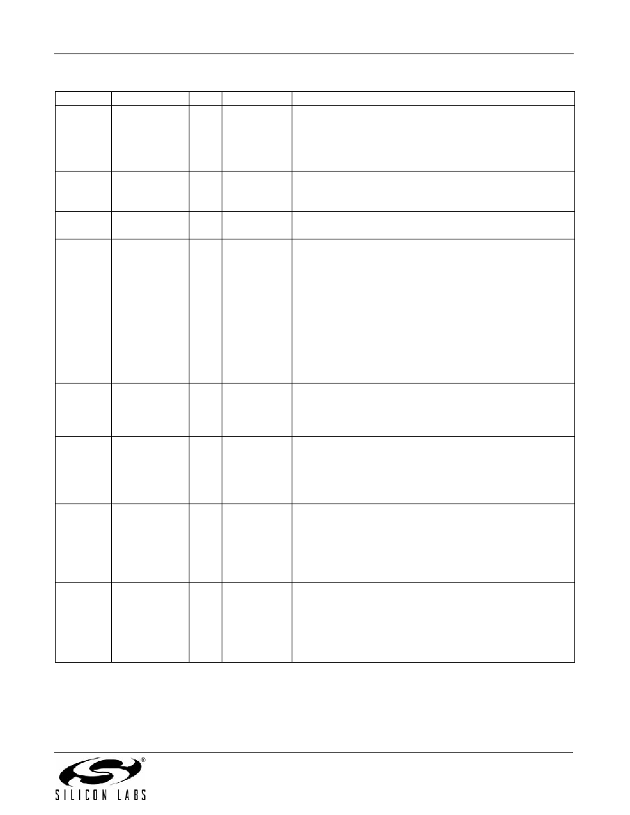
Si5317
Rev. 1.1
37
7
6
XB
XA
I
Analog
External Crystal or Reference Clock.
External crystal should be connected to these pins to use
internal oscillator-based reference. Crystal or reference clock
selection is set by the XTAL/CLOCK pin. See “AN591:
Crystal Selection for the Si5315 and Si5317.”
8,31
GND
Supply
Ground.
Must be connected to system ground. Minimize the ground
path impedance for optimal performance of this device.
11
15
RATE0
RATE1
I
3-Level
External Crystal or Reference Clock Rate.
Note:
See Table 13 for settings.
14
DBL2_BY
I
3-Level
Output 2 Disable/Bypass Mode Control.
Controls enable of CKOUT2 divider/output buffer path and
PLL bypass mode.
L = CKOUT2 enabled
M = CKOUT2 disabled
H = Bypass mode with CKOUT2 enabled
This pin has a weak pull-up and weak pull-down and defaults
to M.
Some designs may require an external resistor voltage
divider when driven by an active device that will tri-state.
Bypass mode is not supported for CMOS clock outputs.
16
17
CKIN+
CKIN–
IMulti
Clock Input.
Differential input clock. This input can also be driven with a
single-ended signal. Input frequency selected from Table 9
18
LOL
O
LVCMOS
PLL Loss of Lock Indicator.
This pin functions as the active high PLL loss of lock indica-
tor.
0 = PLL locked
1 = PLL unlocked
19
DEC
I
LVCMOS
Skew Decrement.
This edge-triggered pin decreases the input to output device
skew. There is no limit on the range of skew adjustment by
this method. Detailed operations and timing characteristics
This pin has a weak pull-down.
20
INC
I
LVCMOS
Skew Increment.
This edge-triggered pin increases the input to output device
skew. There is no limit on the range of skew adjustment by
this method. Detailed operations and timing characteristics
This pin has a weak pull-down.
Table 14. Si5317 Pin Descriptions (Continued)
Pin #
Pin Name
I/O
Signal Level
Description
相关PDF资料 |
PDF描述 |
|---|---|
| SI5320-H-BL | IC CLOCK MULT SONET/SDH 63-PBGA |
| SI5320-H-GL | IC CLOCK MULT SONET/SDH 63LFBGA |
| SI5321-G-BC | IC PREC CLOCK MULTIPLIER 63CBGA |
| SI5321-H-BL | IC CLOCK MULT SONET/SDH 63-PBGA |
| SI5322-B-GM | IC PREC CLOCK MULTIPLIER 36QFN |
相关代理商/技术参数 |
参数描述 |
|---|---|
| SI5317A-C-GMR | 功能描述:时钟合成器/抖动清除器 Pin-Program Jitter Clean Clk 1In/2Out RoHS:否 制造商:Skyworks Solutions, Inc. 输出端数量: 输出电平: 最大输出频率: 输入电平: 最大输入频率:6.1 GHz 电源电压-最大:3.3 V 电源电压-最小:2.7 V 封装 / 箱体:TSSOP-28 封装:Reel |
| Si5317B-C-GM | 功能描述:标准时钟振荡器 Pin-Program. Jitter Cleaning Clock RoHS:否 制造商:AVX 产品:Standard Clock Oscillators 封装 / 箱体:7 mm x 5 mm 频率:75 MHz 频率稳定性:50 PPM 电源电压:2.5 V 负载电容: 端接类型:SMD/SMT 最小工作温度:0 C 最大工作温度:+ 70 C 输出格式:LVDS 尺寸: 封装:Reel 系列: |
| SI5317B-C-GMR | 功能描述:时钟合成器/抖动清除器 Pin-Program Jitter Clean Clk 1In/2Out RoHS:否 制造商:Skyworks Solutions, Inc. 输出端数量: 输出电平: 最大输出频率: 输入电平: 最大输入频率:6.1 GHz 电源电压-最大:3.3 V 电源电压-最小:2.7 V 封装 / 箱体:TSSOP-28 封装:Reel |
| Si5317C-C-GM | 功能描述:标准时钟振荡器 Pin-Program. Jitter Cleaning Clock RoHS:否 制造商:AVX 产品:Standard Clock Oscillators 封装 / 箱体:7 mm x 5 mm 频率:75 MHz 频率稳定性:50 PPM 电源电压:2.5 V 负载电容: 端接类型:SMD/SMT 最小工作温度:0 C 最大工作温度:+ 70 C 输出格式:LVDS 尺寸: 封装:Reel 系列: |
| SI5317C-C-GMR | 功能描述:时钟合成器/抖动清除器 Pin-Program Jitter Clean Clk 1In/2Out RoHS:否 制造商:Skyworks Solutions, Inc. 输出端数量: 输出电平: 最大输出频率: 输入电平: 最大输入频率:6.1 GHz 电源电压-最大:3.3 V 电源电压-最小:2.7 V 封装 / 箱体:TSSOP-28 封装:Reel |
发布紧急采购,3分钟左右您将得到回复。