- 您现在的位置:买卖IC网 > PDF目录2108 > SI5317A-C-GM (Silicon Laboratories Inc)IC CLK JITTER CLEANR PROG 36QFN PDF资料下载
参数资料
| 型号: | SI5317A-C-GM |
| 厂商: | Silicon Laboratories Inc |
| 文件页数: | 32/46页 |
| 文件大小: | 0K |
| 描述: | IC CLK JITTER CLEANR PROG 36QFN |
| 应用说明: | SI5315/17 Crystal Selection AppNote |
| 特色产品: | Si5317 Jitter Cleaning Clock |
| 标准包装: | 490 |
| 系列: | DSPLL® |
| 类型: | 抖动消除器 |
| PLL: | 带旁路 |
| 输入: | 时钟,晶体 |
| 输出: | CML,CMOS,LVDS,LVPECL |
| 电路数: | 1 |
| 比率 - 输入:输出: | 1:2 |
| 差分 - 输入:输出: | 是/是 |
| 频率 - 最大: | 710MHz |
| 除法器/乘法器: | 无/无 |
| 电源电压: | 1.71 V ~ 3.63 V |
| 工作温度: | -40°C ~ 85°C |
| 安装类型: | 表面贴装 |
| 封装/外壳: | 36-VFQFN 裸露焊盘 |
| 供应商设备封装: | 36-QFN(6x6) |
| 包装: | 托盘 |
| 产品目录页面: | 628 (CN2011-ZH PDF) |
| 其它名称: | 336-1923 |
第1页第2页第3页第4页第5页第6页第7页第8页第9页第10页第11页第12页第13页第14页第15页第16页第17页第18页第19页第20页第21页第22页第23页第24页第25页第26页第27页第28页第29页第30页第31页当前第32页第33页第34页第35页第36页第37页第38页第39页第40页第41页第42页第43页第44页第45页第46页
Si5317
38
Rev. 1.1
23
22
BWSEL1
BWSEL0
I
3-Level
Loop Bandwidth Select.
Three level inputs that select the DSPLL closed loop band-
width. See Table 9 on page 22 for available settings.
These pins have both weak pull-ups and weak pull-downs
and default to M.
Some designs may require an external resistor voltage
divider when driven by an active device that will tri-state.
27
26
25
24
FRQSEL3
FRQSEL2
FRQSEL1
FRQSEL0
Frequency Select.
Three level inputs that select the input clock and clock range.
See Table 9 on page 22.
These pins have both weak pull-ups and weak pull-downs
and default to M.
Some designs may require an external resistor voltage
divider when driven by an active device that will tri-state.
29
28
CKOUT1–
CKOUT1+
OMulti
Clock Output 1.
Output signal format is selected by SFOUT pins. Differential
formats supported for LVPECL, LVDS, and CML compatible
modes. For single-ended CMOS format, both output pins
drive identical, in-phase clock outputs.
33
30
SFOUT0
SFOUT1
I
3-Level
Signal Format Select.
Three-level inputs that select the output signal format (com-
mon mode voltage and differential swing) for both CKOUT1
and CKOUT2.
These pins have both weak pull-ups and weak pull-downs
and default to M.
Some designs may require an external resistor voltage
divider when driven by an active device that will tri-state.*
CMOS outputs do not support bypass mode.
34
35
CKOUT2–
CKOUT2+
OMulti
Clock Output 2.
Output signal format is selected by SFOUT pins. Differential
formats supported for LVPECL, LVDS, and CML compatible
modes. For single-ended CMOS format, both output pins
drive identical, in-phase clock outputs.
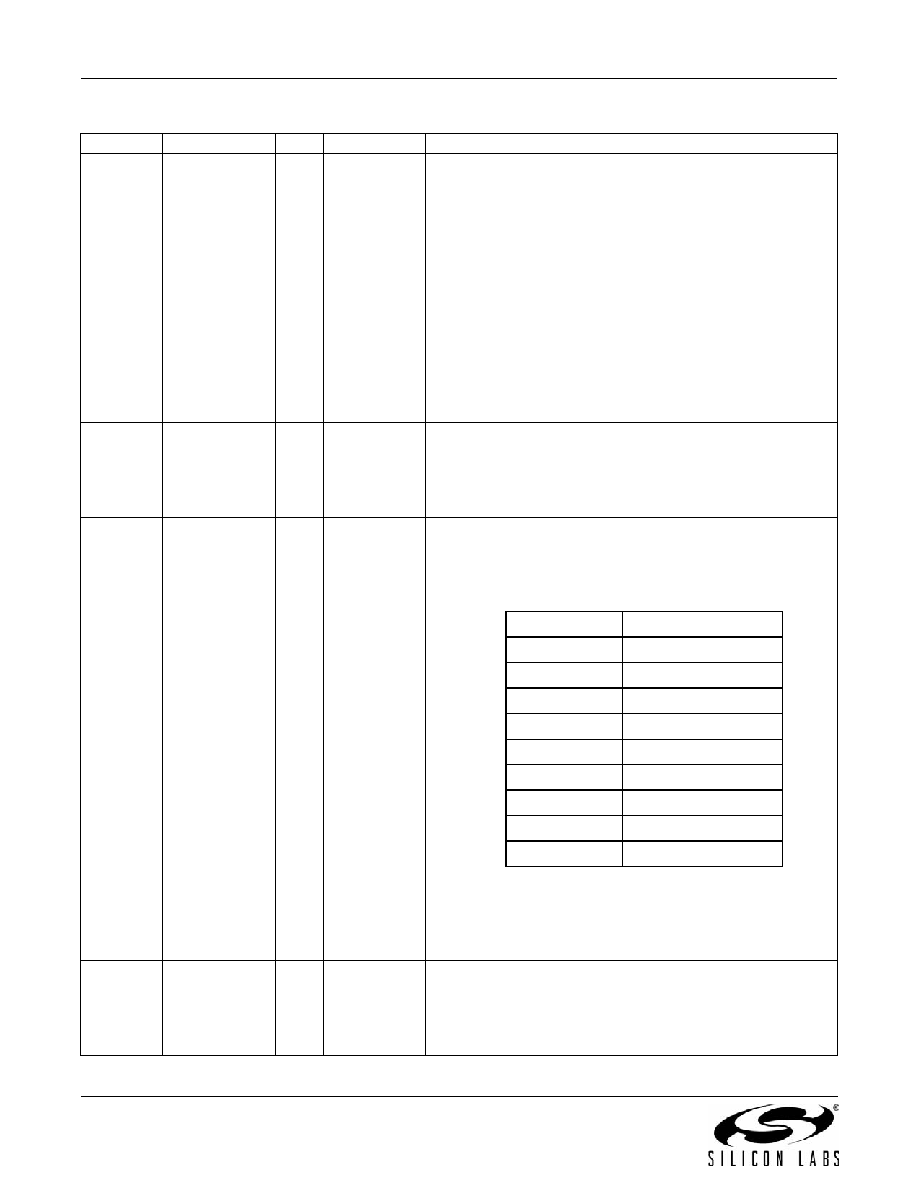
Table 14. Si5317 Pin Descriptions (Continued)
Pin #
Pin Name
I/O
Signal Level
Description
SFOUT[1:0]
Signal Format
HH
Reserved
HM
LVDS
HL
CML
MH
LVPECL
MM
Reserved
ML
LVDS—Low Swing
LH
CMOS
LM
Disable
LL
Reserved
相关PDF资料 |
PDF描述 |
|---|---|
| SI5320-H-BL | IC CLOCK MULT SONET/SDH 63-PBGA |
| SI5320-H-GL | IC CLOCK MULT SONET/SDH 63LFBGA |
| SI5321-G-BC | IC PREC CLOCK MULTIPLIER 63CBGA |
| SI5321-H-BL | IC CLOCK MULT SONET/SDH 63-PBGA |
| SI5322-B-GM | IC PREC CLOCK MULTIPLIER 36QFN |
相关代理商/技术参数 |
参数描述 |
|---|---|
| SI5317A-C-GMR | 功能描述:时钟合成器/抖动清除器 Pin-Program Jitter Clean Clk 1In/2Out RoHS:否 制造商:Skyworks Solutions, Inc. 输出端数量: 输出电平: 最大输出频率: 输入电平: 最大输入频率:6.1 GHz 电源电压-最大:3.3 V 电源电压-最小:2.7 V 封装 / 箱体:TSSOP-28 封装:Reel |
| Si5317B-C-GM | 功能描述:标准时钟振荡器 Pin-Program. Jitter Cleaning Clock RoHS:否 制造商:AVX 产品:Standard Clock Oscillators 封装 / 箱体:7 mm x 5 mm 频率:75 MHz 频率稳定性:50 PPM 电源电压:2.5 V 负载电容: 端接类型:SMD/SMT 最小工作温度:0 C 最大工作温度:+ 70 C 输出格式:LVDS 尺寸: 封装:Reel 系列: |
| SI5317B-C-GMR | 功能描述:时钟合成器/抖动清除器 Pin-Program Jitter Clean Clk 1In/2Out RoHS:否 制造商:Skyworks Solutions, Inc. 输出端数量: 输出电平: 最大输出频率: 输入电平: 最大输入频率:6.1 GHz 电源电压-最大:3.3 V 电源电压-最小:2.7 V 封装 / 箱体:TSSOP-28 封装:Reel |
| Si5317C-C-GM | 功能描述:标准时钟振荡器 Pin-Program. Jitter Cleaning Clock RoHS:否 制造商:AVX 产品:Standard Clock Oscillators 封装 / 箱体:7 mm x 5 mm 频率:75 MHz 频率稳定性:50 PPM 电源电压:2.5 V 负载电容: 端接类型:SMD/SMT 最小工作温度:0 C 最大工作温度:+ 70 C 输出格式:LVDS 尺寸: 封装:Reel 系列: |
| SI5317C-C-GMR | 功能描述:时钟合成器/抖动清除器 Pin-Program Jitter Clean Clk 1In/2Out RoHS:否 制造商:Skyworks Solutions, Inc. 输出端数量: 输出电平: 最大输出频率: 输入电平: 最大输入频率:6.1 GHz 电源电压-最大:3.3 V 电源电压-最小:2.7 V 封装 / 箱体:TSSOP-28 封装:Reel |
发布紧急采购,3分钟左右您将得到回复。