- 您现在的位置:买卖IC网 > PDF目录8973 > SI5338H-A-GM (Silicon Laboratories Inc)IC CLK GEN I2C BUS PROG 24QFN PDF资料下载
参数资料
| 型号: | SI5338H-A-GM |
| 厂商: | Silicon Laboratories Inc |
| 文件页数: | 6/44页 |
| 文件大小: | 0K |
| 描述: | IC CLK GEN I2C BUS PROG 24QFN |
| 标准包装: | 490 |
| 系列: | MultiSynth™ |
| 类型: | * |
| PLL: | 是 |
| 输入: | CML,HCSL,HSCL,LVDS,LVPECL,晶体 |
| 输出: | CMOS,HCSL. HSTL. LVDS. LVPECL. SSTL |
| 电路数: | 1 |
| 比率 - 输入:输出: | 1:4 |
| 差分 - 输入:输出: | 是/是 |
| 频率 - 最大: | 350MHz |
| 除法器/乘法器: | 是/是 |
| 电源电压: | 1.71 V ~ 3.63 V |
| 工作温度: | -40°C ~ 85°C |
| 安装类型: | 表面贴装 |
| 封装/外壳: | 24-VFQFN 裸露焊盘 |
| 供应商设备封装: | 24-QFN(4x4) |
| 包装: | 托盘 |
第1页第2页第3页第4页第5页当前第6页第7页第8页第9页第10页第11页第12页第13页第14页第15页第16页第17页第18页第19页第20页第21页第22页第23页第24页第25页第26页第27页第28页第29页第30页第31页第32页第33页第34页第35页第36页第37页第38页第39页第40页第41页第42页第43页第44页
Si5338
14
Rev. 1.3
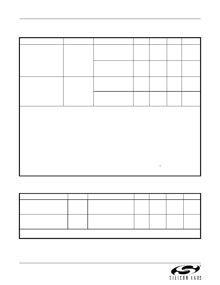
Deterministic Jitter
DJ
Output MultiSynth
operated in fractional
mode7
—3
15
ps pk-pk
Output MultiSynth
operated in integer
mode7
—2
10
ps pk-pk
Total Jitter
(12kHz–20MHz)
TJ =DJ+14xRJ
(See Note 9)
Output MultiSynth
operated in fractional
mode7
—
13
36
ps pk-pk
Output MultiSynth
operated in integer
mode7
—
12
20
ps pk-pk
Table 13. itter Specifications, Clock Buffer Mode (PLL Bypass)*
(VDD = 1.8 V –5% to +10%, 2.5 V ±10%, or 3.3 V ±10%, TA = –40 to 85 °C)
Parameter
Symbol
Test Condition
Min
Typ
Max
Unit
Additive Phase Jitter
(12kHz–20MHz)
tRPHASE
0.7 V pk-pk differential input
clock at 622.08 MHz with
70 ps rise/fall time
—
0.165
—
ps RMS
Additive Phase Jitter
(50kHz–80MHz)
tRPHASEWB
0.7 V pk-pk differential input
clock at 622.08 MHz with
70 ps rise/fall time
—
0.225
—
ps RMS
*Note: All outputs are in Clock Buffer mode (PLL Bypass).
Table 12. Jitter Specifications1,2,3 (Continued)
(VDD = 1.8 V –5% to +10%, 2.5 V ±10%, or 3.3 V ±10%, TA = –40 to 85 °C)
Parameter
Symbol
Test Condition
Min
Typ
Max
Unit
Notes:
1. All jitter measurements apply for LVDS/HCSL/LVPECL/CML output format with a low noise differential input clock and
are made with an Agilent 90804 oscilloscope. All RJ measurements use RJ/DJ separation.
2. For best jitter performance, keep the single ended clock input slew rates at Pins 3 and 4 more than 1.0 V/ns and the
differential clock input slew rates more than 0.3 V/ns.
3. All jitter data in this table is based upon all output formats being differential. When single-ended outputs are used, there
is the potential that the output jitter may increase due to the nature of single-ended outputs. If your configuration
implements any single-ended output and any output is required to have jitter less than 3 ps rms, contact Silicon Labs
for support to validate your configuration and ensure the best jitter performance. In many configurations, CMOS
outputs have little to no effect upon jitter.
4. DJ for PCI and GbE is < 5 ps pp
5. Output MultiSynth in Integer mode.
6. All output clocks 100 MHz HCSL format. Jitter is from the PCIE jitter filter combination that produces the highest jitter.
See AN562 for details. Jitter is measured with the Intel Clock Jitter Tool, Ver. 1.6.4.
7. Input frequency to the Phase Detector between 25 and 40 MHz and any output frequency > 5MHz.
8. Measured in accordance with JEDEC standard 65.
9. Rj is multiplied by 14; estimate the pp jitter from Rj over 212 rising edges.
相关PDF资料 |
PDF描述 |
|---|---|
| MS3454W14S-9S | CONN RCPT 2POS JAM NUT W/SCKT |
| SI5338E-A-GM | IC CLK GEN I2C BUS PROG 24QFN |
| JN1KS10PL2 | CONN RCPT 10POS W/O PIN WALL MT |
| MS27468E17A55S | CONN RCPT 55POS JAM NUT W/SCKT |
| VE-JTY-MZ-F1 | CONVERTER MOD DC/DC 3.3V 16.5W |
相关代理商/技术参数 |
参数描述 |
|---|---|
| SI5338H-A-GMR | 功能描述:时钟发生器及支持产品 I2C-Program Clk Gen 0.16-350MHz inc/dec RoHS:否 制造商:Silicon Labs 类型:Clock Generators 最大输入频率:14.318 MHz 最大输出频率:166 MHz 输出端数量:16 占空比 - 最大:55 % 工作电源电压:3.3 V 工作电源电流:1 mA 最大工作温度:+ 85 C 安装风格:SMD/SMT 封装 / 箱体:QFN-56 |
| SI5338H-B00191-GMR | 制造商:Silicon Laboratories Inc 功能描述:CLOCK - Tape and Reel |
| SI5338H-B00300-GM | 制造商:Silicon Laboratories Inc 功能描述:CLOCK - Bulk |
| SI5338H-B00300-GMR | 制造商:Silicon Laboratories Inc 功能描述:CLOCK - Tape and Reel |
| SI5338H-B00385-GM | 制造商:Silicon Laboratories Inc 功能描述:CLOCK - Bulk |
发布紧急采购,3分钟左右您将得到回复。