- 您现在的位置:买卖IC网 > Datasheet目录511 > SI5402DC-T1-GE3 (Vishay Siliconix)MOSFET N-CH D-S 30V 1206-8 Datasheet资料下载
参数资料
| 型号: | SI5402DC-T1-GE3 |
| 厂商: | Vishay Siliconix |
| 文件页数: | 7/9页 |
| 文件大小: | 0K |
| 描述: | MOSFET N-CH D-S 30V 1206-8 |
| 标准包装: | 3,000 |
| 系列: | TrenchFET® |
| FET 型: | MOSFET N 通道,金属氧化物 |
| FET 特点: | 逻辑电平门 |
| 漏极至源极电压(Vdss): | 30V |
| 电流 - 连续漏极(Id) @ 25° C: | 4.9A |
| 开态Rds(最大)@ Id, Vgs @ 25° C: | 35 毫欧 @ 4.9A,10V |
| Id 时的 Vgs(th)(最大): | 1V @ 250µA |
| 闸电荷(Qg) @ Vgs: | 20nC @ 10V |
| 功率 - 最大: | 1.3W |
| 安装类型: | 表面贴装 |
| 封装/外壳: | 8-SMD,扁平引线 |
| 供应商设备封装: | 1206-8 ChipFET? |
| 包装: | 带卷 (TR) |
�� �
�
�AN811�
�Vishay� Siliconix�
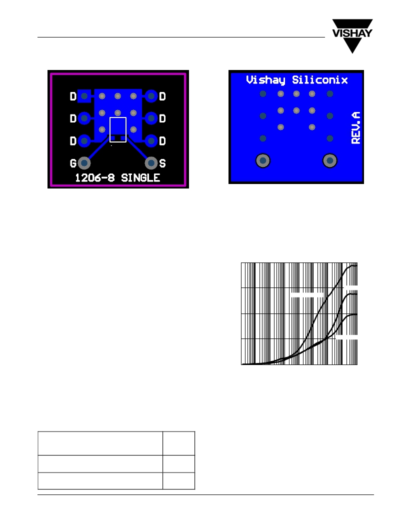
�Front� of� Board�
�ChipFET� r�
�FIGURE� 3.�
�Back� of� Board�
�vishay.com�
�Single� EVB�
�THERMAL� PERFORMANCE�
�Junction-to-Foot� Thermal� Resistance�
�(the� Package� Performance)�
�Thermal� performance� for� the� 1206-8� ChipFET� measured� as�
�junction-to-foot� thermal� resistance� is� 15� _� C/W� typical,� 20� _� C/W�
�maximum� for� the� single� device.� The� “foot”� is� the� drain� lead� of�
�the� device� as� it� connects� with� the� body.� This� is� identical� to� the�
�SO-8� package� R� Q� jf� performance,� a� feat� made� possible� by�
�shortening� the� leads� to� the� point� where� they� become� only� a�
�small� part� of� the� total� footprint� area.�
�The� results� show� that� a� major� reduction� can� be� made� in� the�
�thermal� resistance� by� increasing� the� copper� drain� area.� In� this�
�example,� a� 45� _� C/W� reduction� was� achieved� without� having� to�
�increase� the� size� of� the� board.� If� increasing� board� size� is� an�
�option,� a� further� 33� _� C/W� reduction� was� obtained� by�
�maximizing� the� copper� from� the� drain� on� the� larger� 1”� square�
�pcb.�
�160�
�120�
�Junction-to-Ambient� Thermal� Resistance�
�(dependent� on� pcb� size)�
�The� typical� R� Q� ja� for� the� single-channel� 1206-8� ChipFET� is�
�80� _� C/W� steady� state,� compared� with� 68� _� C/W� for� the� SO-8.�
�Maximum� ratings� are� 95� _� C/W� for� the� 1206-8� versus� 80� _� C/W�
�for� the� SO-8.�
�Testing�
�80�
�40�
�Min.� Footprint�
�1” Square PCB�
�To� aid� comparison� further,� Figure� 4� illustrates� ChipFET� 1206-8�
�thermal� performance� on� two� different� board� sizes� and� three�
�different� pad� patterns.� The� results� display� the� thermal�
�performance� out� to� steady� state� and� produce� a� graphic�
�account� of� how� an� increased� copper� pad� area� for� the� drain�
�connections� can� enhance� thermal� performance.� The�
�measured� steady� state� values� of� R� Q� ja� for� the� single� 1206-8�
�ChipFET� are� :�
�1)� Minimum� recommended� pad� pattern� (see� 156� _� C/W�
�Figure� 2)� on� the� evaluation� board� size� of�
�0.5� in� x� 0.6� in.�
�2)� The� evaluation� board� with� the� pad� pattern� 111� _� C/W�
�described� on� Figure� 3.�
�0�
�10� -5� 10� -4� 10� -3� 10� -2� 10� -1� 1� 10� 100� 1000�
�Time� (Secs)�
�FIGURE� 4.� Single� 1206� ?� 8� ChipFET�
�SUMMARY�
�The� thermal� results� for� the� single-channel� 1206-8� ChipFET�
�package� display� similar� power� dissipation� performance� to� the�
�SO-8� with� a� footprint� reduction� of� 80%.� Careful� design� of� the�
�package� has� allowed� for� this� performance� to� be� achieved.� The�
�short� leads� allow� the� die� size� to� be� maximized� and� thermal�
�resistance� to� be� reduced� within� the� confines� of� the� TSOP-6�
�body� size.�
�ASSOCIATED� DOCUMENT�
�3)� Industry� standard� 1”� square� pcb� with�
�maximum� copper� both� sides.�
�www.vishay.com�
�2�
�78� _� C/W�
�1206-8� ChipFET� Dual� Thermal� performance,� AN812�
�(http://www.vishay.com/doc?71127)� .�
�Document� Number:� 71126�
�12-Dec-03�
�相关PDF资料 |
PDF描述 |
|---|---|
| SI5403DC-T1-GE3 | MOSFET P-CH 30V 6A 1206-8 |
| SI5432DC-T1-GE3 | MOSFET N-CH 20V 6A 1206-8 |
| SI5440DC-T1-GE3 | MOSFET N-CH D-S 30V 1206-8 |
| SI5441DC-T1-GE3 | MOSFET P-CH D-S 20V 1206-8 |
| SI5443DC-T1-GE3 | MOSFET P-CH D-S 20V 1206-8 |
相关代理商/技术参数 |
参数描述 |
|---|---|
| SI5402DC-T2 | 功能描述:MOSFET 30V 6.7A 2.5W 35mohm @ 10V RoHS:否 制造商:STMicroelectronics 晶体管极性:N-Channel 汲极/源极击穿电压:650 V 闸/源击穿电压:25 V 漏极连续电流:130 A 电阻汲极/源极 RDS(导通):0.014 Ohms 配置:Single 最大工作温度: 安装风格:Through Hole 封装 / 箱体:Max247 封装:Tube |
| SI5402DC-T3 | 功能描述:MOSFET 30V 6.7A 2.5W 35mohm @ 10V RoHS:否 制造商:STMicroelectronics 晶体管极性:N-Channel 汲极/源极击穿电压:650 V 闸/源击穿电压:25 V 漏极连续电流:130 A 电阻汲极/源极 RDS(导通):0.014 Ohms 配置:Single 最大工作温度: 安装风格:Through Hole 封装 / 箱体:Max247 封装:Tube |
| SI5403DC | 制造商:VISHAY 制造商全称:Vishay Siliconix 功能描述:P-Channel 30-V (D-S) MOSFET |
| SI5403DC-T1-GE3 | 功能描述:MOSFET 30V 6.0A 6.3W 30mohm @ 10V RoHS:否 制造商:STMicroelectronics 晶体管极性:N-Channel 汲极/源极击穿电压:650 V 闸/源击穿电压:25 V 漏极连续电流:130 A 电阻汲极/源极 RDS(导通):0.014 Ohms 配置:Single 最大工作温度: 安装风格:Through Hole 封装 / 箱体:Max247 封装:Tube |
| SI5404BDC | 制造商:VISHAY 制造商全称:Vishay Siliconix 功能描述:N-Channel 2.5-V (G-S) MOSFET |
发布紧急采购,3分钟左右您将得到回复。