- 您现在的位置:买卖IC网 > PDF目录17725 > SI6404DQ-T1-E3 (Vishay Siliconix)MOSFET N-CH 30V 8.6A 8TSSOP PDF资料下载
参数资料
| 型号: | SI6404DQ-T1-E3 |
| 厂商: | Vishay Siliconix |
| 文件页数: | 6/10页 |
| 文件大小: | 0K |
| 描述: | MOSFET N-CH 30V 8.6A 8TSSOP |
| 标准包装: | 3,000 |
| 系列: | TrenchFET® |
| FET 型: | MOSFET N 通道,金属氧化物 |
| FET 特点: | 逻辑电平门 |
| 漏极至源极电压(Vdss): | 30V |
| 电流 - 连续漏极(Id) @ 25° C: | 8.6A |
| 开态Rds(最大)@ Id, Vgs @ 25° C: | 9 毫欧 @ 11A,10V |
| Id 时的 Vgs(th)(最大): | 600mV @ 250µA |
| 闸电荷(Qg) @ Vgs: | 48nC @ 4.5V |
| 功率 - 最大: | 1.08W |
| 安装类型: | 表面贴装 |
| 封装/外壳: | 8-TSSOP(0.173",4.40mm 宽) |
| 供应商设备封装: | 8-TSSOP |
| 包装: | 带卷 (TR) |
�� �
�
�AN1001�
�Vishay� Siliconix�
�LITTLE� FOOT� R� TSSOP-8�
�The� Next� Step� in� Surface-Mount� Power� MOSFETs�
�Wharton� McDaniel� and� David� Oldham�
�When� Vishay� Siliconix� introduced� its� LITTLE� FOOT�
�MOSFETs,� it� was� the� first� time� that� power� MOSFETs� had� been�
�offered� in� a� true� surface-mount� package,� the� SOIC.� LITTLE�
�FOOT� immediately� found� a� home� in� new� small� form� factor� disk�
�drives,� computers,� and� cellular� phones.�
�The� new� LITTLE� FOOT� TSSOP-8� power� MOSFETs� are� the�
�natural� evolutionary� response� to� the� continuing� demands� of�
�many� markets� for� smaller� and� smaller� packages.� LITTLE�
�FOOT� TSSOP-8� MOSFETs� have� a� smaller� footprint� and� a�
�lower� profile� than� LITTLE� FOOT� SOICs,� while� maintaining� low�
�r� DS(on)� and� high� thermal� performance.� Vishay� Siliconix� has�
�accomplished� this� by� putting� one� or� two� high-density� MOSFET�
�die� in� a� standard� 8-pin� TSSOP� package� mounted� on� a� custom�
�leadframe.�
�THE� TSSOP-8� PACKAGE�
�This� is� the� low� profile� demanded� by� applications� such� as�
�PCMCIA� cards.�
�It� reduces� the� power� package� to� the� same� height� as� many�
�resistors� and� capacitors� in� 0805� and� 0605� sizes.� It� also� allows�
�placement� on� the� “passive”� side� of� the� PC� board.�
�The� standard� pinouts� of� the� LITTLE� FOOT� TSSOP-8�
�packages� have� been� changed� from� the� standard� established�
�by� LITTLE� FOOT.� This� change� minimizes� the� contribution� of�
�interconnection� resistance� to� r� DS(on)� and� maximizes� the�
�transfer� of� heat� out� of� the� package.�
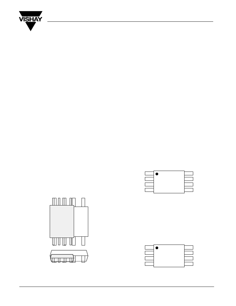
�Figure� 2� shows� the� pinouts� for� a� single-die� TSSOP.� Notice� that�
�both� sides� of� the� package� have� Source� and� Drain�
�connections,� whereas� LITTLE� FOOT� has� the� Source� and� Gate�
�connections� on� one� side� of� the� package,� and� the� Drain�
�connections� are� on� the� opposite� side.�
�LITTLE� FOOT� TSSOP-8� power� MOSFETs� require�
�approximately� half� the� PC� board� area� of� an� equivalent� LITTLE�
�FOOT� device� (Figure� 1).� In� addition� to� the� reduction� in� board�
�area,� the� package� height� has� been� reduced� to� 1.1� mm.�
�Drain�
�Source�
�Source�
�Gate�
�Figure� 2.�
�Pinouts� for� Single� Die� TSSOP�
�Drain�
�Source�
�Source�
�Drain�
�Top� View�
�Figure� 3� shows� the� standard� pinouts� for� a� dual-die� TSSOP-8.�
�In� this� case,� the� connections� for� each� individual� MOSFET�
�occupy� one� side.�
�Drain� 1�
�Drain� 2�
�Side� View�
�Source� 1�
�Source� 1�
�Gate� 1�
�Source� 2�
�Source� 2�
�Gate� 2�
�Figure� 1.�
�An� TSSOP-8� Package� Next� to� a� SOIC-8� Package�
�with� Views� from� Both� Top� and� Side�
�Figure� 3.�
�Pinouts� for� Dual-Die� TSSOP�
�Document� Number:� 70571�
�12-Dec-03�
�www.vishay.com�
�1�
�相关PDF资料 |
PDF描述 |
|---|---|
| MB2411S1W01-HC | SWITCH PUSHBUTTON SPDT 3A 125V |
| SFELF10M7FA00-A0 | FILTER 10.7MHZ 280KHZ BAND RADIA |
| L4K212BJ104MD-T | CAP ARRAY 4CH 0.1UF 10V 0805 |
| 3386Y-1-503LF | TRIMMER 50K OHM 0.5W TH |
| MB2411S1W01-HB | SWITCH PUSHBUTTON SPDT 3A 125V |
相关代理商/技术参数 |
参数描述 |
|---|---|
| SI6404DQ-T1-GE3 | 功能描述:MOSFET 30V 11A 1.75W 9.0mohm @ 10V RoHS:否 制造商:STMicroelectronics 晶体管极性:N-Channel 汲极/源极击穿电压:650 V 闸/源击穿电压:25 V 漏极连续电流:130 A 电阻汲极/源极 RDS(导通):0.014 Ohms 配置:Single 最大工作温度: 安装风格:Through Hole 封装 / 箱体:Max247 封装:Tube |
| SI6405DQ | 制造商:VISHAY 制造商全称:Vishay Siliconix 功能描述:P-Channel 12-V (D-S) MOSFET |
| SI6410DQ | 功能描述:MOSFET 30V/20V NCh MOSFET RoHS:否 制造商:STMicroelectronics 晶体管极性:N-Channel 汲极/源极击穿电压:650 V 闸/源击穿电压:25 V 漏极连续电流:130 A 电阻汲极/源极 RDS(导通):0.014 Ohms 配置:Single 最大工作温度: 安装风格:Through Hole 封装 / 箱体:Max247 封装:Tube |
| SI6410DQ-T1 | 功能描述:MOSFET 30V 7.8A 1.5W RoHS:否 制造商:STMicroelectronics 晶体管极性:N-Channel 汲极/源极击穿电压:650 V 闸/源击穿电压:25 V 漏极连续电流:130 A 电阻汲极/源极 RDS(导通):0.014 Ohms 配置:Single 最大工作温度: 安装风格:Through Hole 封装 / 箱体:Max247 封装:Tube |
| SI6410DQ-T1-E3 | 功能描述:MOSFET 30V 7.8A 1.5W RoHS:否 制造商:STMicroelectronics 晶体管极性:N-Channel 汲极/源极击穿电压:650 V 闸/源击穿电压:25 V 漏极连续电流:130 A 电阻汲极/源极 RDS(导通):0.014 Ohms 配置:Single 最大工作温度: 安装风格:Through Hole 封装 / 箱体:Max247 封装:Tube |
发布紧急采购,3分钟左右您将得到回复。