- 您现在的位置:买卖IC网 > Datasheet目录513 > SI7898DP-T1-GE3 (Vishay Siliconix)MOSFET N-CH 150V 3A PPAK 8SOIC Datasheet资料下载
参数资料
| 型号: | SI7898DP-T1-GE3 |
| 厂商: | Vishay Siliconix |
| 文件页数: | 1/8页 |
| 文件大小: | 0K |
| 描述: | MOSFET N-CH 150V 3A PPAK 8SOIC |
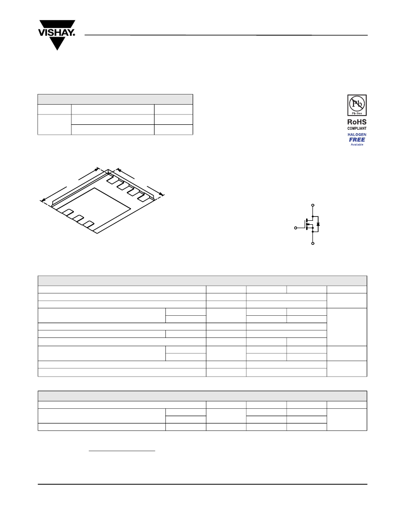
| 产品目录绘图: | DP-T1-(G)E3 Series 8-SOIC |
| 标准包装: | 1 |
| FET 型: | MOSFET N 通道,金属氧化物 |
| FET 特点: | 逻辑电平门 |
| 漏极至源极电压(Vdss): | 150V |
| 电流 - 连续漏极(Id) @ 25° C: | 3A |
| 开态Rds(最大)@ Id, Vgs @ 25° C: | 85 毫欧 @ 3.5A,10V |
| Id 时的 Vgs(th)(最大): | 4V @ 250µA |
| 闸电荷(Qg) @ Vgs: | 21nC @ 10V |
| 功率 - 最大: | 1.9W |
| 安装类型: | 表面贴装 |
| 封装/外壳: | PowerPAK? SO-8 |
| 供应商设备封装: | PowerPAK? SO-8 |
| 包装: | 标准包装 |
| 产品目录页面: | 1663 (CN2011-ZH PDF) |
| 其它名称: | SI7898DP-T1-GE3DKR |
�� �
�
�Si7898DP�
�Vishay� Siliconix�
�N-Channel� 150-V� (D-S)� MOSFET�
�PRODUCT� SUMMARY�
�FEATURES�
�V� DS� (V)�
�150�
�R� DS(on)� (� Ω� )�
�0.085� at� V� GS� =� 10� V�
�0.095� at� V� GS� =� 6.0� V�
�I� D� (A)�
�4.8�
�4.5�
�?� Halogen-free� According� to� IEC� 61249-2-21�
�Available�
�?� TrenchFET� ?� Power� MOSFETs�
�for� Fast� Switching�
�?� New� Low� Thermal� Resistance� PowerPAK� ?�
�Package� with� Low� 1.07� mm� Profile�
�?� PWM� Optimized�
�PowerPAK� SO-8�
�?� 100� %� R� g� Tested�
�APPLICATIONS�
�6.15� mm�
�1�
�S�
�S�
�5.15� mm�
�?� DC/DC� Power� Supply� Primary� Side� Switch�
�2�
�3�
�S�
�4�
�G�
�?� Industrial� Motor� Drives�
�D�
�D�
�8�
�7�
�D�
�D�
�6�
�5�
�D�
�G�
�Bottom� V� ie� w�
�S�
�Ordering� Information:� Si7898DP-T1-E3� (Lead� (Pb)-free)�
�Si7898DP-T1-GE3� (Lead� (Pb)-free� and� Halogen-free)�
�ABSOLUTE� MAXIMUM� RATINGS� T� A� =� 25� °C,� unless� otherwise� noted�
�N-Channel� MOSFET�
�Parameter�
�Drain-Source� Voltage�
�Gate-Source� Voltage�
�Symbol�
�V� DS�
�V� GS�
�10� s�
�Steady� State�
�150�
�±� 20�
�Unit�
�V�
�Continuous� Drain� Current� (T� J� =� 150� °C)� a�
�Pulsed� Drain� Current�
�Avalanche� Current�
�Continuous� Source� Current� (Diode� Conduction)� a�
�T� A� =� 25� °C�
�T� A� =� 70� °C�
�L� =� 0.1� mH�
�I� D�
�I� DM�
�I� AS�
�I� S�
�4.8�
�3.8�
�4.1�
�25�
�10�
�3.0�
�2.4�
�1.6�
�A�
�Maximum� Power� Dissipation� a�
�Operating� Junction� and� Storage� Temperature� Range�
�Soldering� Recommendations� (Peak� Temperature)� b,c�
�T� A� =� 25� °C�
�T� A� =� 70� °C�
�P� D�
�T� J� ,� T� stg�
�5.0�
�3.2�
�-� 55� to� 150�
�260�
�1.9�
�1.2�
�W�
�°C�
�THERMAL� RESISTANCE� RATINGS�
�Parameter�
�Symbol�
�Typical�
�Maximum�
�Unit�
�Maximum� Junction-to-Ambient� a�
�Maximum� Junction-to-Case� (Drain)�
�t� ≤� 10� s�
�Steady� State�
�Steady� State�
�R� thJA�
�R� thJC�
�20�
�52�
�2.1�
�25�
�65�
�2.6�
�°C/W�
�Notes:�
�a.� Surface� Mounted� on� 1"� x� 1"� FR4� board.�
�b.� See� Solder� Profile� (� www.vishay.com/ppg?73257� ).� The� PowerPAK� SO-8� is� a� leadless� package.� The� end� of� the� lead� terminal� is� exposed� copper�
�(not� plated)� as� a� result� of� the� singulation� process� in� manufacturing.� A� solder� fillet� at� the� exposed� copper� tip� cannot� be� guaranteed� and� is� not�
�required� to� ensure� adequate� bottom� side� solder� interconnection.�
�c.� Rework� Conditions:� manual� soldering� with� a� soldering� iron� is� not� recommended� for� leadless� components.�
�Document� Number:� 71873�
�S09-0227-Rev.� D,� 09-Feb-09�
�www.vishay.com�
�1�
�相关PDF资料 |
PDF描述 |
|---|---|
| SI7904BDN-T1-GE3 | MOSFET N-CH DL 20V PPAK 1212-8 |
| SI7905DN-T1-E3 | MOSFET DUAL P-CH D-S 40V 1212-8 |
| SI7913DN-T1-GE3 | MOSFET P-CH 20V 1212-8 PPAK |
| SI7922DN-T1-GE3 | MOSFET DL N-CH 100V PPAK 1212-8 |
| SI7923DN-T1-GE3 | MOSFET P-CH D-S 30V 1212-8 PPAK |
相关代理商/技术参数 |
参数描述 |
|---|---|
| SI78XX | 制造商:SECOS 制造商全称:SeCoS Halbleitertechnologie GmbH 功能描述:3-Terminal Positive Voltage Regulator |
| SI7900 | 制造商:VISHAY 制造商全称:Vishay Siliconix 功能描述:Specification Comparison |
| SI7900AEDN | 制造商:VISHAY 制造商全称:Vishay Siliconix 功能描述:Dual N-Channel 20-V (D-S) MOSFET, Common Drain |
| SI7900AEDN_08 | 制造商:VISHAY 制造商全称:Vishay Siliconix 功能描述:Dual N-Channel 20-V (D-S) MOSFET, Common Drain |
| SI7900AEDN-T1 | 制造商:VISHAY 制造商全称:Vishay Siliconix 功能描述:Dual N-Channel 20-V (D-S) MOSFET, Common Drain |
发布紧急采购,3分钟左右您将得到回复。