- 您现在的位置:买卖IC网 > Datasheet目录514 > SIA814DJ-T1-GE3 (Vishay Siliconix)MOSFET N-CH 30V 4.5A SC70-6 Datasheet资料下载
参数资料
| 型号: | SIA814DJ-T1-GE3 |
| 厂商: | Vishay Siliconix |
| 文件页数: | 2/12页 |
| 文件大小: | 0K |
| 描述: | MOSFET N-CH 30V 4.5A SC70-6 |
| 产品目录绘图: | Mosfet SC70-6, SC75-6 Package |
| 标准包装: | 1 |
| FET 型: | MOSFET N 通道,金属氧化物 |
| FET 特点: | 二极管(隔离式) |
| 漏极至源极电压(Vdss): | 30V |
| 电流 - 连续漏极(Id) @ 25° C: | 4.5A |
| 开态Rds(最大)@ Id, Vgs @ 25° C: | 61 毫欧 @ 3.3A,10V |
| Id 时的 Vgs(th)(最大): | 1.5V @ 250µA |
| 闸电荷(Qg) @ Vgs: | 11nC @ 10V |
| 输入电容 (Ciss) @ Vds: | 340pF @ 10V |
| 功率 - 最大: | 6.5W |
| 安装类型: | 表面贴装 |
| 封装/外壳: | PowerPAK? SC-70-6 双 |
| 供应商设备封装: | PowerPAK? SC-70-6 双 |
| 包装: | 标准包装 |
| 产品目录页面: | 1661 (CN2011-ZH PDF) |
| 其它名称: | SIA814DJ-T1-GE3DKR |
�� �
�
�New� Product�
�SiA814DJ�
�Vishay� Siliconix�
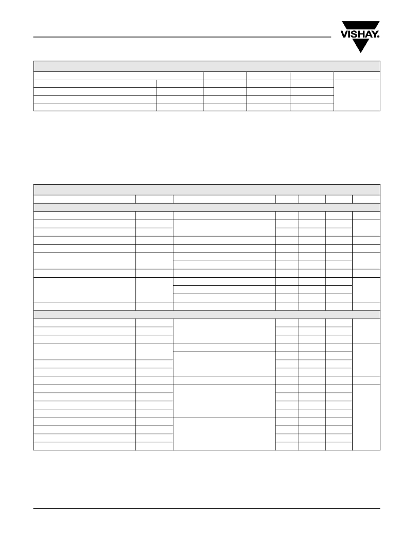
�THERMAL� RESISTANCE� RATINGS�
�Parameter�
�Symbol�
�Typical�
�Maximum�
�Unit�
�Maximum� Junction-to-Ambient� (MOSFET)� b,� f�
�t� ≤� 5s�
�R� thJA�
�52�
�65�
�Maximum� Junction-to-Case� (Drain)� (MOSFET)�
�Maximum� Junction-to-Ambient� (Schottky)� b,� g�
�Maximum� Junction-to-Case� (Drain)� (Schottky)�
�Steady� State�
�t� ≤� 5s�
�Steady� State�
�R� thJC�
�R� thJA�
�R� thJC�
�12.5�
�62�
�15�
�16�
�76�
�18.5�
�°C/W�
�Notes:�
�a.� Package� limited.�
�b.� Surface� Mounted� on� 1"� x� 1"� FR4� board.�
�c.� t� =� 5� s.�
�d.� See� Solder� Profile� (� h� ttp://www.vishay.com/ppg?73257� ).� The� PowerPAK� SC-70� is� a� leadless� package.� The� end� of� the� lead� terminal� is� exposed�
�copper� (not� plated)� as� a� result� of� the� singulation� process� in� manufacturing.� A� solder� fillet� at� the� exposed� copper� tip� cannot� be� guaranteed� and�
�is� not� required� to� ensure� adequate� bottom� side� solder� interconnection.�
�e.� Rework� Conditions:� manual� soldering� with� a� soldering� iron� is� not� recommended� for� leadless� components.�
�f.� Maximum� under� Steady� State� conditions� is� 110� °C/W.�
�g.� Maximum� under� Steady� State� conditions� is� 110� °C/W.�
�SPECIFICATIONS� T� J� =� 25� °C,� unless� otherwise� noted�
�Parameter�
�Symbol�
�Test� Conditions�
�Min.�
�Typ.�
�Max.�
�Unit�
�Static�
�Drain-Source� Breakdown� Voltage�
�V� DS� Temperature� Coefficient�
�V� GS(th)� Temperature� Coefficient�
�V� DS�
�Δ� V� DS� /T� J�
�Δ� V� GS(th)� /T� J�
�V� GS� =� 0� V,� I� D� =� 250� μA�
�I� D� =� 250� μA�
�30�
�27�
�-� 3.7�
�V�
�mV/°C�
�Gate-Source� Threshold� Voltage�
�V� GS(th)�
�V� DS� =� V� GS� ,� I� D� =� 250� μA�
�0.6�
�1.5�
�V�
�Gate-Source� Leakage�
�Zero� Gate� Voltage� Drain� Current�
�On-State� Drain� Current� a�
�I� GSS�
�I� DSS�
�I� D(on)�
�V� DS� =� 0� V,� V� GS� =� ±� 12� V�
�V� DS� =� 30� V,� V� GS� =� 0� V�
�V� DS� =� 30� V,� V� GS� =� 0� V,� T� J� =� 55� °C�
�V� DS� ≥� 5� V,� V� GS� =� 10� V�
�V� GS� =� 10� V,� I� D� =� 3.3� A�
�15�
�0.050�
�±� 100�
�1�
�10�
�0.061�
�nA�
�μA�
�A�
�Drain-Source� On-State� Resistance� a�
�R� DS(on)�
�V� GS� =� 4.5� V,� I� D� =� 3.1� A�
�0.059�
�0.072�
�Ω�
�V� GS� =� 2.5� V,� I� D� =� 0.9� A�
�0.090�
�0.110�
�Forward� Transconductance� a�
�g� fs�
�V� DS� =� 15� V,� I� D� =� 3.3� A�
�9�
�S�
�Dynamic� b�
�Input� Capacitance�
�C� iss�
�340�
�Output� Capacitance�
�Reverse� Transfer� Capacitance�
�C� oss�
�C� rss�
�V� DS� =� 10� V,� V� GS� =� 0� V,� f� =� 1� MHz�
�45�
�25�
�pF�
�Total� Gate� Charge�
�Gate-Source� Charge�
�Q� g�
�Q� gs�
�V� DS� =� 15� V,� V� GS� =� 10� V,� I� D� =� 4.3� A�
�V� DS� =� 15� V,� V� GS� =� 4.5� V,� I� D� =� 4.3� A�
�7�
�3.2�
�0.9�
�11�
�5�
�nC�
�Gate-Drain� Charge�
�Q� gd�
�0.8�
�Gate� Resistance�
�Turn-On� Delay� Time�
�Rise� Time�
�Turn-Off� DelayTime�
�R� g�
�t� d(on)�
�t� r�
�t� d(off)�
�f� =� 1� MHz�
�V� DD� =� 15� V,� R� L� =� 4.3� Ω�
�I� D� ?� 3.5� A,� V� GEN� =� 4.5� V,� R� g� =� 1� Ω�
�2�
�10�
�10�
�15�
�15�
�15�
�25�
�Ω�
�Fall� Time�
�Turn-On� Delay� Time�
�t� f�
�t� d(on)�
�10�
�5�
�15�
�10�
�ns�
�Rise� Time�
�Turn-Off� DelayTime�
�Fall� Time�
�t� r�
�t� d(off)�
�t� f�
�V� DD� =� 15� V,� R� L� =� 4.3� Ω�
�I� D� ?� 3.5� A,� V� GEN� =� 10� V,� R� g� =� 1� Ω�
�12�
�15�
�10�
�20�
�25�
�15�
�www.vishay.com�
�2�
�Document� Number:� 68672�
�S-81176-Rev.� A,� 26-May-08�
�相关PDF资料 |
PDF描述 |
|---|---|
| SIA911EDJ-T1-GE3 | MOSFET P-CH DL 20V PWRPAK SC70-6 |
| SIA914DJ-T1-GE3 | MOSFET DL N-CH 20V PPAK SC70-6 |
| SIA917DJ-T1-GE3 | MOSFET P-CH DL 20V PWRPAK SC70-6 |
| SIB406EDK-T1-GE3 | MOSFET N-CH D-S 20V SC-75-6 |
| SIB408DK-T1-GE3 | MOSFET N-CH D-S 30V PPAK SC75-6L |
相关代理商/技术参数 |
参数描述 |
|---|---|
| SiA817EDJ-T1-GE3 | 功能描述:MOSFET -30V .065Ohm@10V 4.5A P-Ch G-III RoHS:否 制造商:STMicroelectronics 晶体管极性:N-Channel 汲极/源极击穿电压:650 V 闸/源击穿电压:25 V 漏极连续电流:130 A 电阻汲极/源极 RDS(导通):0.014 Ohms 配置:Single 最大工作温度: 安装风格:Through Hole 封装 / 箱体:Max247 封装:Tube |
| SIA850DJ-T1-GE3 | 功能描述:MOSFET 190V 0.95A 7.0W RoHS:否 制造商:STMicroelectronics 晶体管极性:N-Channel 汲极/源极击穿电压:650 V 闸/源击穿电压:25 V 漏极连续电流:130 A 电阻汲极/源极 RDS(导通):0.014 Ohms 配置:Single 最大工作温度: 安装风格:Through Hole 封装 / 箱体:Max247 封装:Tube |
| SI-A8W031180EU | 制造商:Samsung 功能描述:Bulk |
| SI-A8W032180EU | 制造商:Samsung 功能描述:Bulk |
| SI-A8W041140EU | 制造商:Samsung 功能描述:Bulk |
发布紧急采购,3分钟左右您将得到回复。