- 您现在的位置:买卖IC网 > PDF目录85251 > SL28540ALC (SILICON LABORATORIES) OTHER CLOCK GENERATOR, QCC56 PDF资料下载
参数资料
| 型号: | SL28540ALC |
| 厂商: | SILICON LABORATORIES |
| 元件分类: | 时钟产生/分配 |
| 英文描述: | OTHER CLOCK GENERATOR, QCC56 |
| 封装: | 8 X 8 MM, LEAD FREE, QFN-56 |
| 文件页数: | 4/25页 |
| 文件大小: | 267K |
| 代理商: | SL28540ALC |
SL28540
Rev 1.2, September 15, 2008
Page 12 of 25
PD_RESTORE
If a ‘0’ is set for Byte 0 bit 0 then, upon assertion of PWRDWN#
LOW, the SL28540 initiates a full reset. The result of this is that
the clock chip emulates a cold power on start and goes to the
“Latches Open” state. If the PD_RESTORE bit is set to a ‘1’
then the configuration is stored upon PWRDWN# asserted
LOW. Note that if the iAMT bit, Byte 0 bit 3, is set to a ‘1’ then
the PD_RESTORE bit must be ignored. In other words, in Intel
iAMT mode, PWRDWN# reset is not allowed.
PWRDWN# (Power down) Clarification
The CKPWRGD/PWRDWN# pin is a dual-function pin. During
initial power up, the pin functions as CKPWRGD. Once
CKPWRGD has been sampled HIGH by the clock chip, the pin
assumes PD# functionality. The PD# pin is an asynchronous
active LOW input used to shut off all clocks cleanly before
shutting off power to the device. This signal is synchronized
internally to the device before powering down the clock
synthesizer. PD# is also an asynchronous input for powering
up the system. When PD# is asserted LOW, clocks are driven
to a LOW value and held before turning off the VCOs and the
crystal oscillator.
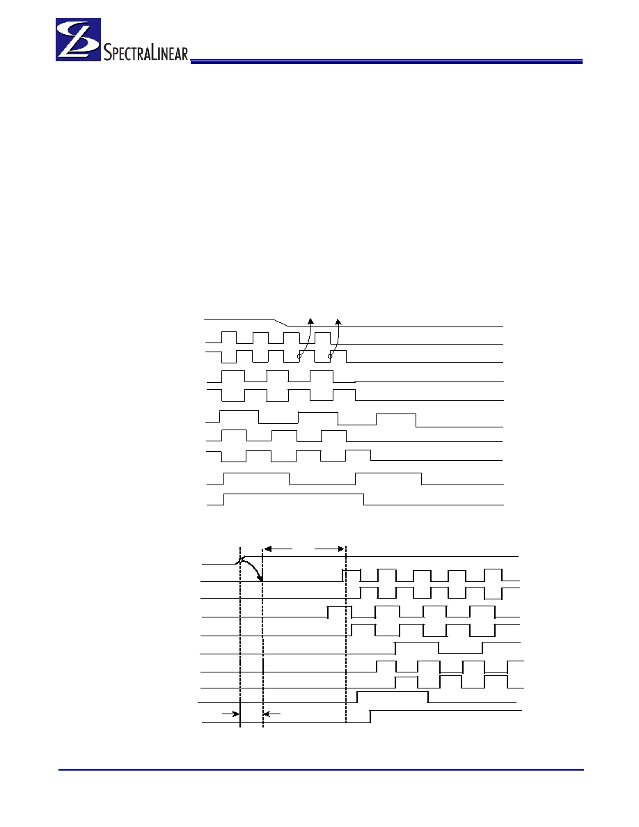
PWRDWN# (Power down) Assertion
When PD is sampled HIGH by two consecutive rising edges
of CPUC, all single-ended outputs will be held LOW on their
next HIGH-to-LOW transition and differential clocks must held
LOW. When PD mode is desired as the initial power on state,
PD must be asserted HIGH in less than 10 s after asserting
CKPWRGD.
PWRDWN# Deassertion
The power up latency is less than 1.8 ms. This is the time from
the deassertion of the PD# pin or the ramping of the power
supply until the time that stable clocks are generated from the
clock chip. All differential outputs stopped in a three-state
condition, resulting from power down are driven high in less
than 300 s of PD# deassertion to a voltage greater than
200 mV. After the clock chip’s internal PLL is powered up and
locked, all outputs are enabled within a few clock cycles of
each clock. Figure 4 is an example showing the relationship of
clocks coming up.
PD#
USB, 48MHz
DOT96T
DOT96C
SRCT 100MHz
SRCC 100MHz
CPUT, 133MHz
PCI, 33 MHz
REF
CPUC, 133MHz
Figure 3. Power down Assertion Timing Waveform
D OT 9 6 C
PD#
C P U C , 1 3 3 MH z
C P U T , 1 3 3 MH z
S R C C 1 0 0 MH z
U S B , 4 8 MH z
D OT 9 6 T
S R C T 1 0 0 MH z
Ts ta b le
< 1 .8 m s
P C I, 3 3 MH z
REF
Td r iv e _ PW R D N #
< 3 0 0 s , > 2 0 0 m V
Figure 4. Power down Deassertion Timing Waveform
相关PDF资料 |
PDF描述 |
|---|---|
| S83C154UFXXX-36:D | 8-BIT, MROM, 36 MHz, MICROCONTROLLER, PQCC44 |
| S83C154UFXXX-40:R | 8-BIT, MROM, 40 MHz, MICROCONTROLLER, PQCC44 |
| S83C154UFXXX-42:D | 8-BIT, MROM, 42 MHz, MICROCONTROLLER, PQCC44 |
| S912XDP512J1MAL | 16-BIT, FLASH, 40 MHz, MICROCONTROLLER, PQFP112 |
| S912XDP512F0CALR | 16-BIT, FLASH, 40 MHz, MICROCONTROLLER, PQFP112 |
相关代理商/技术参数 |
参数描述 |
|---|---|
| SL28540ALCT | 功能描述:时钟发生器及支持产品 Low Power for Intel Mobile RoHS:否 制造商:Silicon Labs 类型:Clock Generators 最大输入频率:14.318 MHz 最大输出频率:166 MHz 输出端数量:16 占空比 - 最大:55 % 工作电源电压:3.3 V 工作电源电流:1 mA 最大工作温度:+ 85 C 安装风格:SMD/SMT 封装 / 箱体:QFN-56 |
| SL28541BQCR | 功能描述:时钟发生器及支持产品 Montevina, Atom RoHS:否 制造商:Silicon Labs 类型:Clock Generators 最大输入频率:14.318 MHz 最大输出频率:166 MHz 输出端数量:16 占空比 - 最大:55 % 工作电源电压:3.3 V 工作电源电流:1 mA 最大工作温度:+ 85 C 安装风格:SMD/SMT 封装 / 箱体:QFN-56 |
| SL28541BQCRT | 功能描述:时钟发生器及支持产品 Montevina, Atom RoHS:否 制造商:Silicon Labs 类型:Clock Generators 最大输入频率:14.318 MHz 最大输出频率:166 MHz 输出端数量:16 占空比 - 最大:55 % 工作电源电压:3.3 V 工作电源电流:1 mA 最大工作温度:+ 85 C 安装风格:SMD/SMT 封装 / 箱体:QFN-56 |
| SL28541BZC | 功能描述:时钟发生器及支持产品 Montevina RoHS:否 制造商:Silicon Labs 类型:Clock Generators 最大输入频率:14.318 MHz 最大输出频率:166 MHz 输出端数量:16 占空比 - 最大:55 % 工作电源电压:3.3 V 工作电源电流:1 mA 最大工作温度:+ 85 C 安装风格:SMD/SMT 封装 / 箱体:QFN-56 |
| SL28541BZC-2 | 功能描述:时钟发生器及支持产品 Montevina, Atom RoHS:否 制造商:Silicon Labs 类型:Clock Generators 最大输入频率:14.318 MHz 最大输出频率:166 MHz 输出端数量:16 占空比 - 最大:55 % 工作电源电压:3.3 V 工作电源电流:1 mA 最大工作温度:+ 85 C 安装风格:SMD/SMT 封装 / 箱体:QFN-56 |
发布紧急采购,3分钟左右您将得到回复。