- 您现在的位置:买卖IC网 > PDF目录297406 > SL811HS-JCT (CYPRESS SEMICONDUCTOR CORP) UNIVERSAL SERIAL BUS CONTROLLER, PQCC28 PDF资料下载
参数资料
| 型号: | SL811HS-JCT |
| 厂商: | CYPRESS SEMICONDUCTOR CORP |
| 元件分类: | 总线控制器 |
| 英文描述: | UNIVERSAL SERIAL BUS CONTROLLER, PQCC28 |
| 封装: | LEAD FREE, PLASTIC, LCC-28 |
| 文件页数: | 12/32页 |
| 文件大小: | 854K |
| 代理商: | SL811HS-JCT |
第1页第2页第3页第4页第5页第6页第7页第8页第9页第10页第11页当前第12页第13页第14页第15页第16页第17页第18页第19页第20页第21页第22页第23页第24页第25页第26页第27页第28页第29页第30页第31页第32页
SL811HS
Document 38-08008 Rev. *D
Page 2 of 32
Data Port, Microprocessor Interface
The SL811HS microprocessor interface provides an 8-bit
bidirectional data path along with appropriate control lines to
interface to external processors or controllers. Programmed
I/O or memory mapped I/O designs are supported through the
8-bit interface, chip select, read and write input strobes, and a
single address line, A0.
Access to memory and control register space is a simple two
step process, requiring an address Write with A0 = ’0’, followed
by a register/memory Read or Write cycle with address line A0
= ’1’.
In addition, a DMA bidirectional interface in slave mode is
available with handshake signals such as nDRQ, nDACK,
nWR, nRD, nCS and INTRQ.
The SL811HS WRITE or READ operation terminates when
either nWR or nCS goes inactive. For devices interfacing to
the SL811HS that deactivate the Chip Select nCS before the
Write nWR, the data hold timing must be measured from the
nCS and will be the same value as specified. Therefore, both
Intel- and Motorola-type CPUs work easily with the SL811HS
without any external glue logic requirements.
DMA Controller (slave mode only)
In applications that require transfers of large amounts of data
such as scanner interfaces, the SL811HS provides a DMA in-
terface. This interface supports DMA READ or WRITE trans-
fers to the SL811HS internal RAM buffer, it is done through the
microprocessor data bus via two control lines (nDRQ - Data
Request and nDACK - Data Acknowledge), along with the
nWR line and controls the data flow into the SL811HS. The
SL811HS has a count register that allows selection of pro-
grammable block sizes for DMA transfer. The control signals,
both nDRQ and nDACK, are designed for compatibility with
standard DMA interfaces.
Interrupt Controller
The SL811HS interrupt controller provides a single output
signal (INTRQ) that is activated by a number of programmable
events that may occur as result of USB activity. Control and
status registers are provided to allow the user to select single
or multiple events, which generate an interrupt (assert INTRQ)
and let the user view interrupt status. The interrupts are
cleared by writing to the Interrupt Status Register.
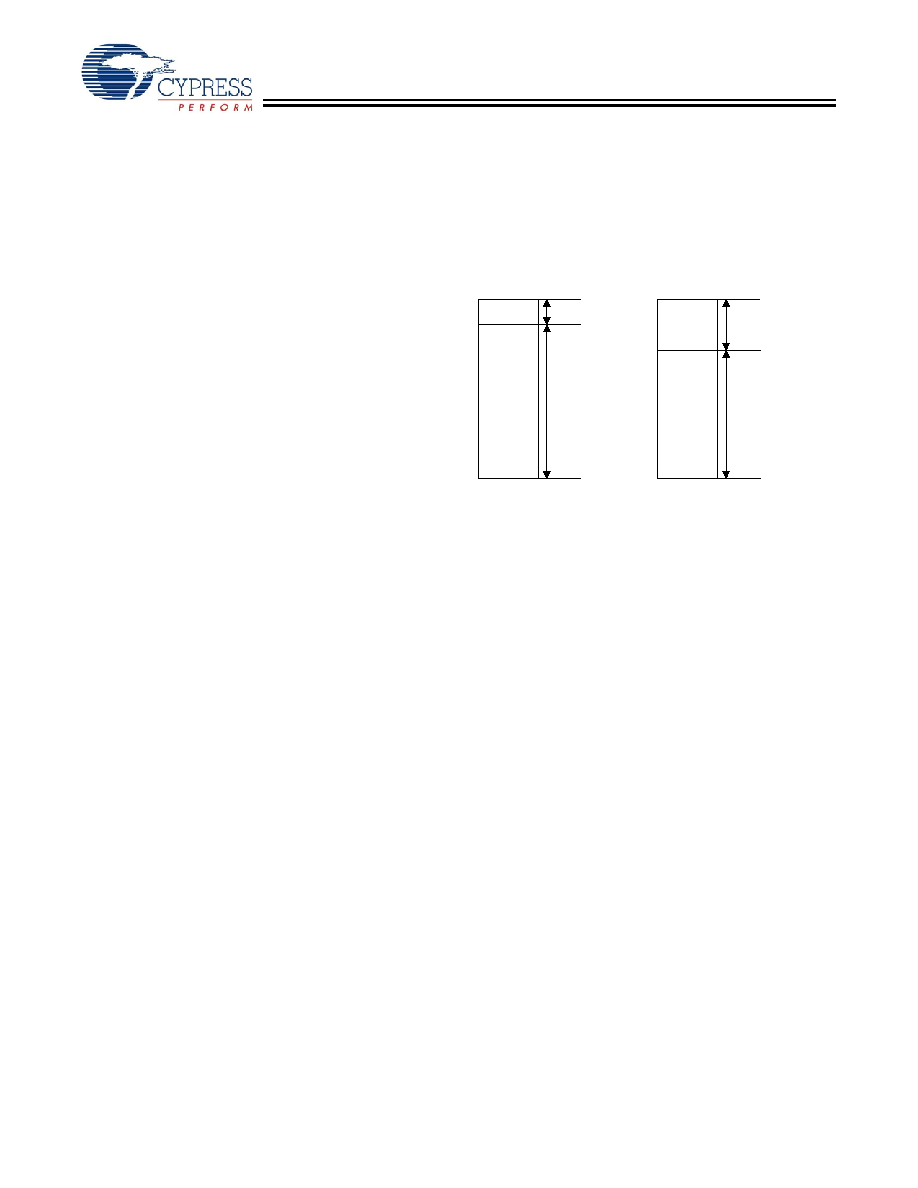
Buffer Memory
The SL811HS contains 256 bytes of internal memory used for
USB data buffers, control registers, and status registers. When
in master mode (host mode), the memory is defined where the
first 16 bytes are registers and the remaining 240 bytes are
used for USB data buffers. When in slave mode (peripheral
mode), the first 64 bytes are used for the four endpoint control
and status registers along with the various other registers. This
leaves 192 bytes of endpoint buffer space for USB data
transfers.
Access to the registers and data memory is through the 8-bit
external microprocessor data bus, in either indexed or direct
addressing. Indexed mode uses the Auto Address Increment
mode described in
direct addressing is used to READ/WRITE to an individual
address.
USB transactions are automatically routed to the memory
buffer that is configured for that transfer. Control registers are
provided so that pointers and block sizes in buffer memory are
determined and allocated.
Auto Address Increment Mode
The SL811HS supports auto increment mode to reduce READ
and WRITE memory cycles. In this mode, the microcontroller
needs to set up the address only once. Whenever any subse-
quent DATA is accessed, the internal address counter advanc-
es to the next address location.
Auto Address Increment Example. To fill the data buffer
that is configured for address 10h, follow these steps:
1. Write 10h to SL811HS with A0 LOW. This sets the memory
address that is used for the next operation.
2. Write the first data byte into address 10h by doing a write
operation with A0 HIGH. An example is a Get Descriptor;
the first byte that is sent to the device is 80h
(bmRequestType) so you would write 80h to address 10h.
3. Now the internal RAM address pointer is set to 11h. So, by
doing another write with A0 HIGH, RAM address location
11h is written with the data. Continuing with the Get
Descriptor example, a 06h is written to address 11h for the
bRequest value.
4. Repeat Step 3 until all the required bytes are written as
necessary for a transfer. If auto-increment is not used, you
write the address value each time before writing the data
as shown in Step 1.
The advantage of auto address increment mode is that it
reduces
the
number
of
required
SL811HS
memory
READ/WRITE cycles to move data to/from the device. For
example, transferring 64 bytes of data to/from SL811HS, using
auto increment mode, reduces the number of cycles to 1
address WRITE and 64 READ/WRITE data cycles, compared
to 64 address writes and 64 data cycles for random access.
0x00 – 0x0F Control
and status registers
0x10 – 0xFF
USB data buffer
240 bytes
16 bytes
0x00 – 0x39
Control/status registers
and endpoint
control/status registers
0x40 – 0xFF
USB data buffer
192 bytes
64 bytes
Host Mode Memory Map
Peripheral Mode Memory Map
Figure 1. Memory Map
相关PDF资料 |
PDF描述 |
|---|---|
| SL811HS | SL811HS Embedded USB Host/Slave Controller(SL811HS嵌入式USB主/从控制器) |
| SLA0201 | 600 V, SCR |
| SLA24C01-D-3/P | The CAT24FC02 is a 2-kb Serial CMOS EEPROM internally organized as 256 words of 8 bits each |
| SLA24C01-D/P | The CAT24FC02 is a 2-kb Serial CMOS EEPROM internally organized as 256 words of 8 bits each |
| SLE24C01-S/P | The CAT24FC02 is a 2-kb Serial CMOS EEPROM internally organized as 256 words of 8 bits each |
相关代理商/技术参数 |
参数描述 |
|---|---|
| SL811HST | 制造商:CYPRESS 制造商全称:Cypress Semiconductor 功能描述:Embedded USB Host/Slave Controller |
| SL811HST-1.5 | 制造商:Cypress Semiconductor 功能描述:BUS Controller Circuit, 48 Pin, QFP |
| SL811HST-AC | 功能描述:IC USB HOST/SLAVE CTRLR 48LQFP RoHS:否 类别:集成电路 (IC) >> 嵌入式 - 微控制器 - 特定应用 系列:- 产品变化通告:Product Discontinuation 26/Aug/2009 标准包装:250 系列:- 应用:网络处理器 核心处理器:4Kc 程序存储器类型:- 控制器系列:- RAM 容量:16K x 8 接口:以太网,UART,USB 输入/输出数:- 电源电压:1.8V, 3.3V 工作温度:- 安装类型:表面贴装 封装/外壳:208-LQFP 包装:带卷 (TR) 供应商设备封装:PG-LQFP-208 其它名称:SP000314382 |
| SL811HST-AXC | 功能描述:USB 接口集成电路 256B HOST COM RoHS:否 制造商:Cypress Semiconductor 产品:USB 2.0 数据速率: 接口类型:SPI 工作电源电压:3.15 V to 3.45 V 工作电源电流: 最大工作温度:+ 85 C 安装风格:SMD/SMT 封装 / 箱体:WLCSP-20 |
| SL811HST-AXC | 制造商:Cypress Semiconductor 功能描述:IC USB HOST CONTROLLER 48MHZ 制造商:Cypress Semiconductor 功能描述:IC, USB HOST CONTROLLER, 48MHZ 制造商:Cypress Semiconductor 功能描述:IC, USB HOST CONTROLLER, 48MHZ; No. of I/O's:8; Digital IC Case Style:TQFP; No. of Pins:48; RAM Memory Size:256KB; CPU Speed:48MHz; Peripherals:DMA; Embedded Interface Type:USB; Operating Temperature Min:0C; Operating Temperature |
发布紧急采购,3分钟左右您将得到回复。