- 您现在的位置:买卖IC网 > PDF目录98084 > SM320C6414DGADW60 (TEXAS INSTRUMENTS INC) 64-BIT, 75 MHz, OTHER DSP, CPGA570 PDF资料下载
参数资料
| 型号: | SM320C6414DGADW60 |
| 厂商: | TEXAS INSTRUMENTS INC |
| 元件分类: | 数字信号处理 |
| 英文描述: | 64-BIT, 75 MHz, OTHER DSP, CPGA570 |
| 封装: | 33 X 33 MM, CERAMIC, FCPGA-570 |
| 文件页数: | 72/134页 |
| 文件大小: | 1997K |
| 代理商: | SM320C6414DGADW60 |
第1页第2页第3页第4页第5页第6页第7页第8页第9页第10页第11页第12页第13页第14页第15页第16页第17页第18页第19页第20页第21页第22页第23页第24页第25页第26页第27页第28页第29页第30页第31页第32页第33页第34页第35页第36页第37页第38页第39页第40页第41页第42页第43页第44页第45页第46页第47页第48页第49页第50页第51页第52页第53页第54页第55页第56页第57页第58页第59页第60页第61页第62页第63页第64页第65页第66页第67页第68页第69页第70页第71页当前第72页第73页第74页第75页第76页第77页第78页第79页第80页第81页第82页第83页第84页第85页第86页第87页第88页第89页第90页第91页第92页第93页第94页第95页第96页第97页第98页第99页第100页第101页第102页第103页第104页第105页第106页第107页第108页第109页第110页第111页第112页第113页第114页第115页第116页第117页第118页第119页第120页第121页第122页第123页第124页第125页第126页第127页第128页第129页第130页第131页第132页第133页第134页
SMJ320C6414, SMJ320C6415, SMJ320C6416
FIXEDPOINT DIGITAL SIGNAL PROCESSORS
SGUS050A JANUARY 2004 REVISED MARCH 2004
42
POST OFFICE BOX 1443
HOUSTON, TEXAS 772511443
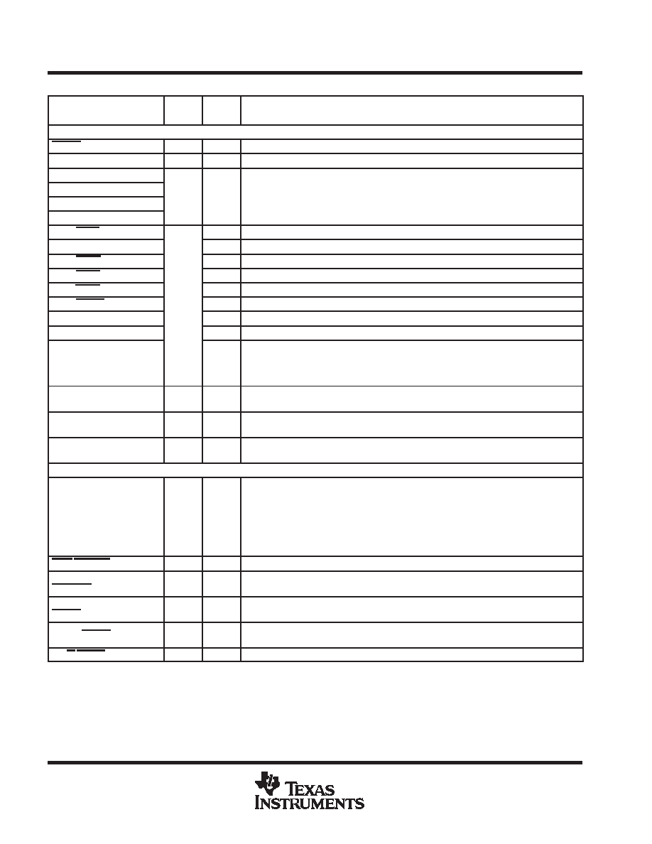
Terminal Functions (Continued)
SIGNAL
TYPE
IPD/
DESCRIPTION
NAME
NO.
TYPE
IPD/
IPU
DESCRIPTION
RESETS, INTERRUPTS, AND GENERAL-PURPOSE INPUT/OUTPUTS
RESET
AB5
I
Device reset
NMI
E6
I
IPD
Nonmaskable interrupt, edge-driven (rising edge)
GP7/EXT_INT7
Y6
General-purpose input/output (GPIO) pins (I/O/Z) or external interrupts (input only). The
default after reset setting is GPIO enabled as input-only.
GP6/EXT_INT6
V8
I/O/Z
IPU
General-purpose input/output (GPIO) pins (I/O/Z) or external interrupts (input only). The
default after reset setting is GPIO enabled as input-only.
When these pins function as External Interrupts [by selecting the corresponding interrupt
GP5/EXT_INT5
AA5
I/O/Z
IPU
When these pins function as External Interrupts [by selecting the corresponding interrupt
enable register bit (IER.[7:4])], they are edge-driven and the polarity can be
GP4/EXT_INT4
U9
enable register bit (IER.[7:4])], they are edge-driven and the polarity can be
independently selected via the External Interrupt Polarity Register bits (EXTPOL.[3:0]).
GP15/PRST§
J8
General-purpose input/output (GPIO) 15 pin (I/O/Z) or PCI reset (I). No function at default.
GP14/PCLK§
G5
GPIO 14 pin (I/O/Z) or PCI clock (I). No function at default.
GP13/PINTA§
G4
GPIO 13 pin (I/O/Z) or PCI interrupt A (O/Z). No function at default.
GP12/PGNT§
J7
GPIO 12 pin (I/O/Z) or PCI bus grant (I). No function at default.
GP11/PREQ§
H6
GPIO 11 pin (I/O/Z) or PCI bus request (O/Z). No function at default.
GP10/PCBE3§
L7
I/O/Z
GPIO 10 pin (I/O/Z) or PCI command/byte enable 3 (I/O/Z). No function at default.
GP9/PIDSEL§
K6
I/O/Z
GPIO 9 pin (I/O/Z) or PCI initialization device select (I). No function at default.
GP3
AA6
IPD
GPIO 3 pin (I/O/Z). The default after reset setting is GPIO 3 enabled as input-only.
GP0
W8
IPD
GPIO 0 pin.
The general-purpose I/O 0 pin (GPIO 0) (I/O/Z) can be programmed as GPIO 0 (input only)
[default] or as GPIO 0 (output only) pin or output as a general-purpose interrupt (GP0INT)
signal (output only).
CLKS2/GP8§
W7
I/O/Z
IPD
McBSP2 external clock source (CLKS2) [input only] [default] or this pin can be pro-
grammed as a GPIO 8 pin (I/O/Z).
CLKOUT6/GP2§
T10
I/O/Z
IPD
Clock output at 1/6 of the device speed (O/Z) [default] or this pin can be programmed as a
GPIO 2 pin (I/O/Z).
CLKOUT4/GP1§
Y7
I/O/Z
IPD
Clock output at 1/4 of the device speed (O/Z) [default] or this pin can be programmed as a
GPIO 1 pin (I/O/Z).
HOST-PORT INTERFACE (HPI) [C64x] or PERIPHERAL COMPONENT INTERCONNECT (PCI) [C6415 or C6416 devices only]
PCI_EN
T8
I
IPD
PCI enable pin. This pin controls the selection (enable/disable) of the HPI and GP[15:9], or
PCI peripherals (for the C6415 and C6416 devices). This pin works in conjunction with the
MCBSP2_EN pin to enable/disable other peripherals (for more details, see the Device Con-
figurations section of this data sheet).
The C6414 device does not support the PCI peripheral; for proper device operation, do not
oppose the internal pulldown (IPD) on this pin.
HINT/PFRAME§
P4
I/O/Z
Host interrupt from DSP to host (O) [default] or PCI frame (I/O/Z)
HCNTL1/
PDEVSEL§
N8
I/O/Z
Host control selects between control, address, or data registers (I) [default] or PCI device
select (I/O/Z).
HCNTL0/
PSTOP§
P5
I/O/Z
Host control selects between control, address, or data registers (I) [default] or PCI stop
(I/O/Z)
HHWIL/PTRDY§
N5
I/O/Z
Host half-word select first or second half-word (not necessarily high or low order)
[For HPI16 bus width selection only] (I) [default] or PCI target ready (I/O/Z)
HR/W/PCBE2§
N6
I/O/Z
Host read or write select (I) [default] or PCI command/byte enable 2 (I/O/Z)
I = Input, O = Output, Z = High impedance, S = Supply voltage, GND = Ground
IPD = Internal pulldown, IPU = Internal pullup. (These IPD/IPU signal pins feature a 30-k IPD or IPU resistor. To pull up a signal to the opposite
supply rail, a 1-k
resistor should be used.)
§ For the C6415 and C6416 devices, these pins are multiplexed pins. For more details, see the Device Configurations section of this data sheet.
The C6414 device does not support the PCI or UTOPIA peripherals; therefore, these MUXed peripheral pins are standalone peripheral functions
for this device.
For the C6414 device, only these pins are multiplexed pins.
相关PDF资料 |
PDF描述 |
|---|---|
| SM320C6416DGADW60 | 64-BIT, 75 MHz, OTHER DSP, CPGA570 |
| SMJ320C6701GLPW16 | 32-BIT, 166.66 MHz, OTHER DSP, CBGA429 |
| SMJ34010-50FDM | GRAPHICS PROCESSOR, CQCC68 |
| SMJ34010-40GBM | GRAPHICS PROCESSOR, CPGA68 |
| SMJ34010FDM | GRAPHICS PROCESSOR, CQCC68 |
相关代理商/技术参数 |
参数描述 |
|---|---|
| SM320C6414-EP | 制造商:TI 制造商全称:Texas Instruments 功能描述:FIXED-POINT DIGITAL SIGNAL PROCESSORS |
| SM320C6415DGADW60 | 制造商:Texas Instruments 功能描述:DSP Fixed-Point 32-Bit 600MHz 4800MIPS 570-Pin FCPGA Tray |
| SM320C6416DGADW60 | 制造商:TI 制造商全称:Texas Instruments 功能描述:FIXD-POINT DIGITAL SIGNAL PROCESSORS |
| SM320C6424GDUQ6EP | 功能描述:数字信号处理器和控制器 - DSP, DSC EP Fixed-Pt Dig Signal Proc RoHS:否 制造商:Microchip Technology 核心:dsPIC 数据总线宽度:16 bit 程序存储器大小:16 KB 数据 RAM 大小:2 KB 最大时钟频率:40 MHz 可编程输入/输出端数量:35 定时器数量:3 设备每秒兆指令数:50 MIPs 工作电源电压:3.3 V 最大工作温度:+ 85 C 封装 / 箱体:TQFP-44 安装风格:SMD/SMT |
| SM320C6455BGTZEP | 功能描述:数字信号处理器和控制器 - DSP, DSC Enh Product Fixed- Pt Dig Signal Proc RoHS:否 制造商:Microchip Technology 核心:dsPIC 数据总线宽度:16 bit 程序存储器大小:16 KB 数据 RAM 大小:2 KB 最大时钟频率:40 MHz 可编程输入/输出端数量:35 定时器数量:3 设备每秒兆指令数:50 MIPs 工作电源电压:3.3 V 最大工作温度:+ 85 C 封装 / 箱体:TQFP-44 安装风格:SMD/SMT |
发布紧急采购,3分钟左右您将得到回复。