- 您现在的位置:买卖IC网 > PDF目录373464 > SN65LVDTS33D (Texas Instruments, Inc.) HIGH-SPEED DIFFERENTIAL RECEIVERS PDF资料下载
参数资料
| 型号: | SN65LVDTS33D |
| 厂商: | Texas Instruments, Inc. |
| 英文描述: | HIGH-SPEED DIFFERENTIAL RECEIVERS |
| 中文描述: | 高速差分接收器 |
| 文件页数: | 4/23页 |
| 文件大小: | 504K |
| 代理商: | SN65LVDTS33D |
www.ti.com
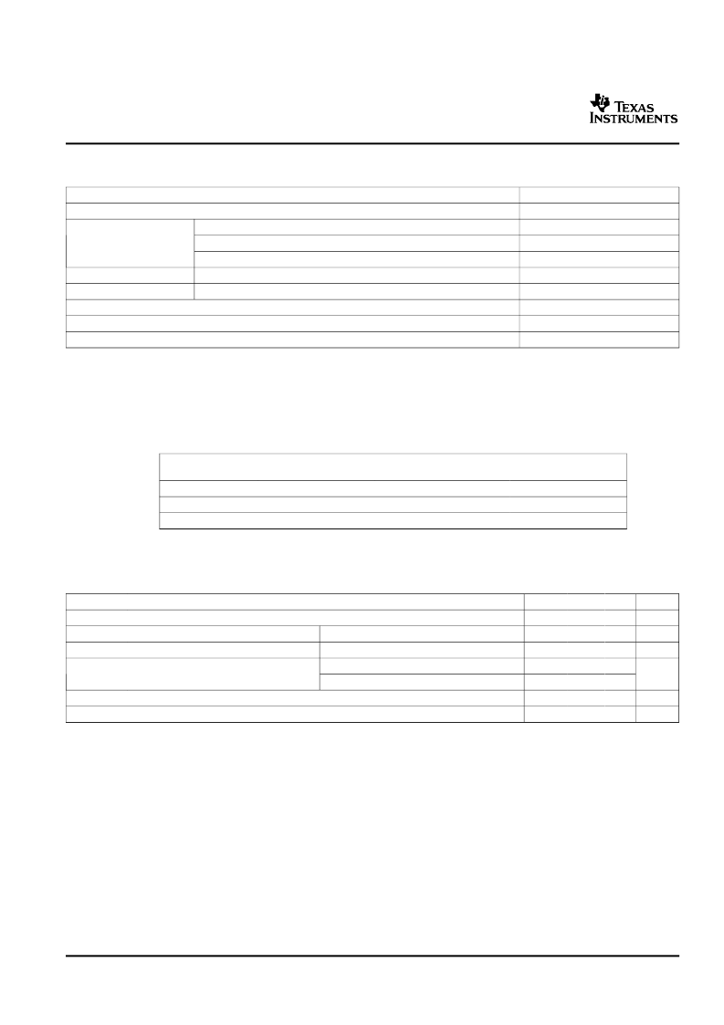
ABSOLUTE MAXIMUM RATINGS
over operating free-air temperature range (unless otherwise noted)
(1)
DISSIPATION RATING TABLE
RECOMMENDED OPERATING CONDITIONS
SN65LVDS33, SN65LVDT33
SN65LVDS34, SN65LVDT34
SLLS490B–MARCH 2001–REVISED NOVEMBER 2004
UNIT
Supply voltage range, V
CC(2)
–0.5 V to 4 V
–1 V to 6 V
–5 V to 6 V
1 V
Enables or Y
A or B
|V
A
– V
B
| (LVDT)
A, B, and GND
(3)
All pins
(4)
Voltage range
Electrostatic discharge
Charged-device mode
Continuous power dissipation
Storage temperature range
Lead temperature 1,6 mm (1/16 inch) from case for 10 seconds
Class 3, A: 15 kV, B: 500 V
±500 V
See Dissipation Rating Table
–65°C to 150°C
260°C
(1)
Stresses beyond those listed under
absolute maximum ratings
may cause permanent damage to the device. These are stress ratings
only, and functional operation of the device at these or any other conditions beyond those indicated under
recommended operating
conditions
is not implied. Exposure to absolute-maximum-rated conditions for extended periods may affect device reliability.
All voltage values, except differential I/O bus voltages, are with respect to network ground terminal.
Tested in accordance with JEDEC Standard 22, Test Method A114-A.
Tested in accordance with JEDEC Standard 22, Test Method C101.
(2)
(3)
(4)
T
≤
25°C
POWER RATING
725 mW
774 mW
950 mW
OPERATING FACTOR
(1)
ABOVE T
A
= 25°C
5.8 mW/°C
6.2 mW/°C
7.6 mW/°C
T
= 85°C
POWER RATING
377 mW
402 mW
494 mW
PACKAGE
D8
PW16
D16
(1)
This is the inverse of the junction-to-ambient thermal resistance when board-mounted and with no air
flow.
MIN
NOM
3.3
MAX
3.6
UNIT
V
V
V
V
CC
V
IH
V
IL
Supply voltage
High-level input voltage
Low-level input voltage
3
2
0
Enables
Enables
LVDS
LVDT
5
0.8
0.1
3
| V
ID
|
Magnitude of differential input voltage
V
0.8
V
I
or V
IC
T
A
Voltage at any bus terminal (separately or common-mode)
Operating free-air temperature
–4
5
V
°C
–40
85
4
Submit Documentation Feedback
相关PDF资料 |
PDF描述 |
|---|---|
| SN7400DRE4 | QUADRUPLE 2-INPUT POSITIVE-NAND GATES |
| SN7400DRG4 | QUADRUPLE 2-INPUT POSITIVE-NAND GATES |
| SN7400NSRE4 | QUADRUPLE 2-INPUT POSITIVE-NAND GATES |
| SN7400NSRG4 | QUADRUPLE 2-INPUT POSITIVE-NAND GATES |
| SN7404NSRE4 | HEX INVERTERS |
相关代理商/技术参数 |
参数描述 |
|---|---|
| SN65LVEL11D | 功能描述:时钟缓冲器 3.3V PECL 1:2 Fanout Buffer RoHS:否 制造商:Texas Instruments 输出端数量:5 最大输入频率:40 MHz 传播延迟(最大值): 电源电压-最大:3.45 V 电源电压-最小:2.375 V 最大功率耗散: 最大工作温度:+ 85 C 最小工作温度:- 40 C 封装 / 箱体:LLP-24 封装:Reel |
| SN65LVEL11DGK | 功能描述:时钟缓冲器 3.3V PECL 1:2 Fanout Buffer RoHS:否 制造商:Texas Instruments 输出端数量:5 最大输入频率:40 MHz 传播延迟(最大值): 电源电压-最大:3.45 V 电源电压-最小:2.375 V 最大功率耗散: 最大工作温度:+ 85 C 最小工作温度:- 40 C 封装 / 箱体:LLP-24 封装:Reel |
| SN65LVEL11DGKR | 功能描述:时钟缓冲器 3.3V PECL 1:2 Fanout Buffer RoHS:否 制造商:Texas Instruments 输出端数量:5 最大输入频率:40 MHz 传播延迟(最大值): 电源电压-最大:3.45 V 电源电压-最小:2.375 V 最大功率耗散: 最大工作温度:+ 85 C 最小工作温度:- 40 C 封装 / 箱体:LLP-24 封装:Reel |
| SN65LVEL11DR | 功能描述:时钟缓冲器 3.3V PECL 1:2 Fanout Buffer RoHS:否 制造商:Texas Instruments 输出端数量:5 最大输入频率:40 MHz 传播延迟(最大值): 电源电压-最大:3.45 V 电源电压-最小:2.375 V 最大功率耗散: 最大工作温度:+ 85 C 最小工作温度:- 40 C 封装 / 箱体:LLP-24 封装:Reel |
| SN65LVELT22D | 功能描述:转换 - 电压电平 3.3V Dual LVTTL to Diff LVPECL Trans RoHS:否 制造商:Micrel 类型:CML/LVDS/LVPECL to LVCMOS/LVTTL 传播延迟时间:1.9 ns 电源电流:14 mA 电源电压-最大:3.6 V 电源电压-最小:3 V 最大工作温度:+ 85 C 安装风格:SMD/SMT 封装 / 箱体:MLF-8 |
发布紧急采购,3分钟左右您将得到回复。