- 您现在的位置:买卖IC网 > PDF目录365666 > SN74V3660-15PEU (Texas Instruments, Inc.) 3.3-V CMOS FIRST-IN, FIRST-OUT MEMORIES PDF资料下载
参数资料
| 型号: | SN74V3660-15PEU |
| 厂商: | Texas Instruments, Inc. |
| 英文描述: | 3.3-V CMOS FIRST-IN, FIRST-OUT MEMORIES |
| 中文描述: | 的3.3V的CMOS先入先出存储器 |
| 文件页数: | 5/50页 |
| 文件大小: | 729K |
| 代理商: | SN74V3660-15PEU |
第1页第2页第3页第4页当前第5页第6页第7页第8页第9页第10页第11页第12页第13页第14页第15页第16页第17页第18页第19页第20页第21页第22页第23页第24页第25页第26页第27页第28页第29页第30页第31页第32页第33页第34页第35页第36页第37页第38页第39页第40页第41页第42页第43页第44页第45页第46页第47页第48页第49页第50页
SN74V3640, SN74V3650, SN74V3660, SN74V3670, SN74V3680, SN74V3690
1024
×
36, 2048
×
36, 4096
×
36, 8192
×
36, 16384
×
36, 32768
×
36
3.3-V CMOS FIRST-IN, FIRST-OUT MEMORIES
SCAS668A
–
NOVEMBER 2001
–
REVISED MARCH 2003
5
POST OFFICE BOX 655303
DALLAS, TEXAS 75265
description (continued)
If the asynchronous PAE/PAF configuration is selected, PAE is asserted low on the low-to-high transition of
RCLK. PAE is reset to high on the low-to-high transition of WCLK. Similarly, PAF is asserted low on the
low-to-high transition of WCLK, and PAF is reset to high on the low-to-high transition of RCLK.
If the synchronous PAE/PAF configuration is selected , the PAE is asserted and updated on the rising edge of
RCLK only, and not WCLK. Similarly, PAF is asserted and updated on the rising edge of WCLK only, and not
RCLK. The mode desired is configured during master reset by the state of the programmable flag mode (PFM).
The retransmit function allows data to be reread from the FIFO more than once. A low on the retransmit (RT)
input during a rising RCLK edge initiates a retransmit operation by setting the read pointer to the first location
of the memory array. Zero-latency retransmit timing mode can be selected using the retransmit timing mode
(RM). During master reset, a low on RM selects zero-latency retransmit. A high on RM during master reset
selects normal latency.
If zero-latency retransmit operation is selected, the first data word to be retransmitted is placed on the output
register, with respect to the same RCLK edge that initiated the retransmit, if RT is low.
See Figures 11 and 12 for normal latency retransmit timing. See Figures 13 and 14 for zero-latency retransmit
timing.
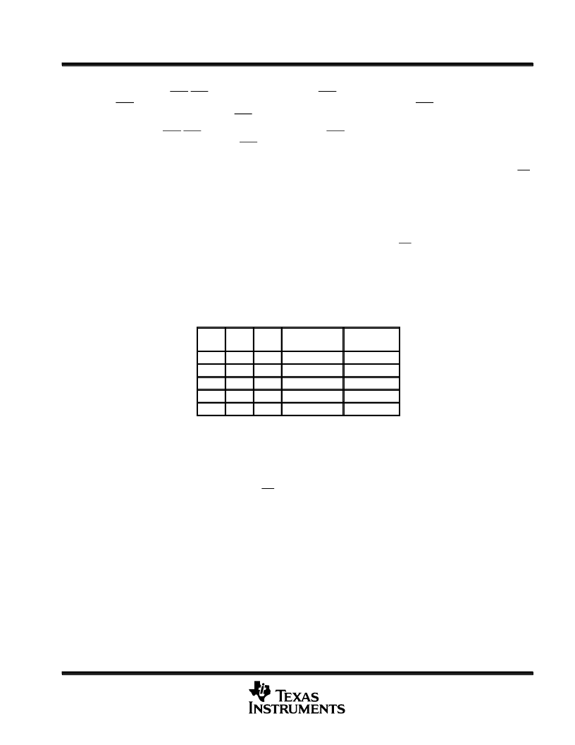
The devices can be configured with different input and output bus widths (see Table 1).
Table 1. Bus-Matching Configuration Modes
BM
IW
OW
WRITE-PORT
WIDTH
READ-PORT
WIDTH
L
L
L
×
36
×
36
×
36
×
18
×
9
×
36
×
18
×
9
×
36
×
36
H
L
L
H
L
H
H
H
L
H
H
H
Logic levels during master reset
A big-endian/little-endian data word format is provided. This function is useful when data is written into the FIFO
in long-word (
×
36/
×
18) format and read out of the FIFO in small-word (
×
18/
×
9) format. If big-endian mode is
selected, the most-significant byte (MSB) (word) of the long word written into the FIFO is read out of the FIFO
first, followed by the least-significant byte (LSB). If little-endian format is selected, the LSB of the long word
written into the FIFO is read out first, followed by the MSB. The mode desired is configured during master reset
by the state of the big-endian/little-endian (BE) pin (see Figure 4 for the bus-matching byte arrangement).
The interspersed/noninterspersed parity (IP) bit function allows the user to select the parity bit in the word loaded
into the parallel port (D0
–
Dn) when programming the flag offsets. If interspersed-parity mode is selected, the
FIFO assumes that the parity bit is located in bit positions D8, D17, D26, and D35 during the parallel
programming of the flag offsets. If noninterspersed-parity mode is selected, D8, D17, and D26 are assumed
to be valid bits, and D32, D33, D34, and D35 are ignored. Interspersed parity mode is selected during master
reset by the state of the IP input. Interspersed parity control has an effect only during parallel programming of
the offset registers. It does not affect data written to and read from the FIFO.
The SN74V3640, SN74V3650, SN74V3660, SN74V3670, SN74V3680, and SN74V3690 are fabricated using
high-speed submicron CMOS technology, and are characterized for operation from 0
°
C to 70
°
C.
相关PDF资料 |
PDF描述 |
|---|---|
| SN74V3670-10PEU | 3.3-V CMOS FIRST-IN, FIRST-OUT MEMORIES |
| SN74V3670-15PEU | 3.3-V CMOS FIRST-IN, FIRST-OUT MEMORIES |
| SN74V3690-15PEU | 3.3-V CMOS FIRST-IN, FIRST-OUT MEMORIES |
| SN75108AN | DUAL LINE RECEIVERS |
| SN55107AFK | DUAL LINE RECEIVERS |
相关代理商/技术参数 |
参数描述 |
|---|---|
| SN74V3660-6PEU | 功能描述:先进先出 4096 x 36 Synch 先进先出 Memory RoHS:否 制造商:IDT 电路数量: 数据总线宽度:18 bit 总线定向:Unidirectional 存储容量:4 Mbit 定时类型:Synchronous 组织:256 K x 18 最大时钟频率:100 MHz 访问时间:10 ns 电源电压-最大:3.6 V 电源电压-最小:6 V 最大工作电流:35 mA 最大工作温度:+ 85 C 封装 / 箱体:TQFP-80 封装: |
| SN74V3660-7PEU | 功能描述:先进先出 4096 x 36 Synch 先进先出 Memory RoHS:否 制造商:IDT 电路数量: 数据总线宽度:18 bit 总线定向:Unidirectional 存储容量:4 Mbit 定时类型:Synchronous 组织:256 K x 18 最大时钟频率:100 MHz 访问时间:10 ns 电源电压-最大:3.6 V 电源电压-最小:6 V 最大工作电流:35 mA 最大工作温度:+ 85 C 封装 / 箱体:TQFP-80 封装: |
| SN74V3670-10PEU | 功能描述:先进先出 8192 x 36 Synch 先进先出 Memory RoHS:否 制造商:IDT 电路数量: 数据总线宽度:18 bit 总线定向:Unidirectional 存储容量:4 Mbit 定时类型:Synchronous 组织:256 K x 18 最大时钟频率:100 MHz 访问时间:10 ns 电源电压-最大:3.6 V 电源电压-最小:6 V 最大工作电流:35 mA 最大工作温度:+ 85 C 封装 / 箱体:TQFP-80 封装: |
| SN74V3670-15PEU | 功能描述:先进先出 8192 x 36 Synch 先进先出 Memory RoHS:否 制造商:IDT 电路数量: 数据总线宽度:18 bit 总线定向:Unidirectional 存储容量:4 Mbit 定时类型:Synchronous 组织:256 K x 18 最大时钟频率:100 MHz 访问时间:10 ns 电源电压-最大:3.6 V 电源电压-最小:6 V 最大工作电流:35 mA 最大工作温度:+ 85 C 封装 / 箱体:TQFP-80 封装: |
| SN74V3670-6PEU | 功能描述:先进先出 8192 x 36 Synch 先进先出 Memory RoHS:否 制造商:IDT 电路数量: 数据总线宽度:18 bit 总线定向:Unidirectional 存储容量:4 Mbit 定时类型:Synchronous 组织:256 K x 18 最大时钟频率:100 MHz 访问时间:10 ns 电源电压-最大:3.6 V 电源电压-最小:6 V 最大工作电流:35 mA 最大工作温度:+ 85 C 封装 / 箱体:TQFP-80 封装: |
发布紧急采购,3分钟左右您将得到回复。