- 您现在的位置:买卖IC网 > PDF目录225220 > SP7800AJS 2-CH 12-BIT SUCCESSIVE APPROXIMATION ADC, PARALLEL ACCESS, PDSO24 PDF资料下载
参数资料
| 型号: | SP7800AJS |
| 元件分类: | ADC |
| 英文描述: | 2-CH 12-BIT SUCCESSIVE APPROXIMATION ADC, PARALLEL ACCESS, PDSO24 |
| 封装: | 0.300 INCH, PLASTIC, SOIC-24 |
| 文件页数: | 10/13页 |
| 文件大小: | 171K |
| 代理商: | SP7800AJS |
SP7800ADS/02
SP7800A 12-Bit 3
s Sampling A/D Converter
Copyright 2000 Sipex Corporation
6
OBSOLETE
-
HIST
ORICAL
REFERENCE
ONL
Y
CS
R/C
HBE
BUSY
OPERATION
1
X
1
None – outputs in Hi-Z state.
01
0
1
Holds signal and initiates conversion.
0101
Output three-state buffers enabled once
conversion has finished.
0111
Enable hi-byte in 8-bit bus mode.
01
0
1
Inhibit start of conversion.
0011
None – outputs in Hi-Z state.
X
0
Conversion in progress. Outputs Hi-Z
state. New conversion inhibited until
present conversion has finished.
Table 1. Control Line Functions
onR/C.Thethree-statedataoutputbuffersareenabled
when R/C is HIGH and BUSY is HIGH. Thus, there
are two possible modes of operation: conversion can
be initiated with either positive or negative pulses. In
either case, the R/C pulse must remain LOW a
minimum of 40ns.
Figure 5 illustrates timing when conversion is initi-
ated by an R/C pulse which goes LOW and returns
HIGH during the conversion. In this case (Convert
Mode),thethree-stateoutputsgointotheHi-Zstatein
responsetothefallingedgeofR/C,andareenabledfor
external access to the data after completion of the
conversion.
Figure 6 illustrates the timing when conversion is
initiated by a positive R/C pulse. In this mode (Read
Mode), the output data from the previous conversion
is enabled during the HIGH portion of R/C. A new
conversion starts on the falling edge of R/C, and the
three-stateoutputsreturntotheHi-Zstateuntilthenext
occurrence of a HIGH on R/C.
Conversion Start
A conversion is initiated on the SP7800A only by a
negative transition occurring on R/C, as shown in
Table 2. No other combination of states or transitions
will initiate a conversion. Conversion is inhibited if
either CS or HBE are HIGH, or if BUSY is LOW. CS
andHBEshouldbestableaminimumof25nspriorto
the transition on R/C. Timing relationships for start of
conversion are illustrated in Figure 7.
The BUSY output indicates the current state of the
converter by being LOW only during conversion.
During this time the three-state output buffers remain
in a Hi-Z state, and therefore data cannot be read
during conversion. During this period, additional
transitions on the three digital inputs (CS, R/C and
HBE) will be ignored, so that conversion cannot be
prematurely terminated or restarted.
Internal Clock
The SP7800A has an internal clock that is factory
trimmed to achieve a typical conversion time of
2.6
s, and a maximum conversion time over the
full operating temperature range of 2.7
s. No
external adjustments are required, and with the
guaranteed maximum acquisition time of 300ns,
throughput performance is assured with convert
pulses as close as 3
s.
Reading Data
Afterconversionisinitiated,theoutputbuffersremain
in a Hi-Z state until the following three logic condi-
tions are simultaneously met: R/C is HIGH, BUSY is
HIGH and CS is LOW. Upon satisfying these condi-
tions, the data lines are enabled according to the state
of HBE. See Figure 7 for timing relationships and
specifications.
CALIBRATION...
Optional External Gain And Offset Trim
Offset and full-scale errors may be trimmed to zero
using external offset and full-scale trim potenti-
ometers connected to the SP7800A as shown in
Figure 3.
If adjustment of offset and full scale is not required,
connections as shown in Figure 2 should be used.
Calibration Procedure
Applyaprecisioninputvoltagesourcetoyourchosen
input range (
±10V range at pin1 or ±5V at pin 2). Set
the A/D to convert continuously. Monitor the output
code.Trimtheoffsetfirst,thengain.Usetheappropri-
ate input voltages and output target codes for your
chosen input range as follows. The recommended
offset calibration voltage values eliminate interaction
between the offset and gain calibration.
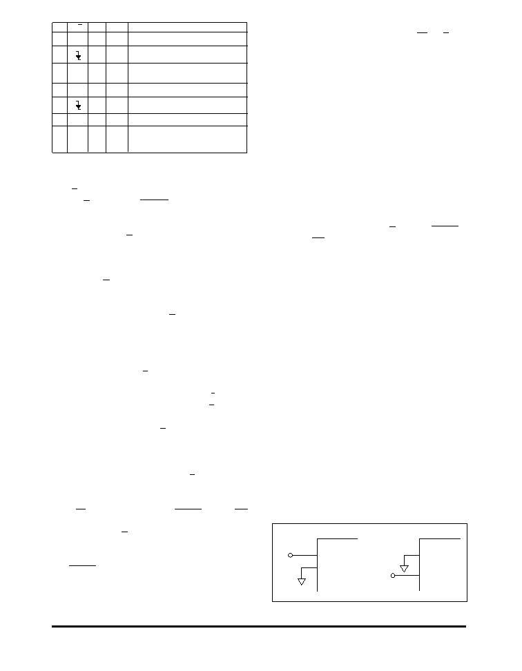
Figure 2. a)
±10V Range b) ±5V Range — Without Trims
1
2
±10V
Input
SP7800A
1
2
±5V
Input
SP7800A
相关PDF资料 |
PDF描述 |
|---|---|
| SP7802SQ/883 | 12-BIT SUCCESSIVE APPROXIMATION ADC, PARALLEL ACCESS, CDIP24 |
| SP809EK-L-2-3 | 1-CHANNEL POWER SUPPLY SUPPORT CKT, PDSO3 |
| SP810EK-2.3/TR | 1-CHANNEL POWER SUPPLY SUPPORT CKT, PDSO3 |
| SP8121BS | 8-CH 12-BIT SUCCESSIVE APPROXIMATION ADC, PARALLEL ACCESS, PDSO32 |
| SP813MCN-L | 1-CHANNEL POWER SUPPLY SUPPORT CKT, PDSO8 |
相关代理商/技术参数 |
参数描述 |
|---|---|
| SP7800AKN | 制造商:SIPEX 制造商全称:Sipex Corporation 功能描述:12-Bit 3ms Sampling A/D Converter |
| SP7800AKS | 制造商:SIPEX 制造商全称:Sipex Corporation 功能描述:12-Bit 3ms Sampling A/D Converter |
| SP7805AIS WAF | 制造商:Texas Instruments 功能描述: |
| SP7805V2-L | 功能描述:DC/DC 开关控制器 30 TERMINAL 1A POS RoHS:否 制造商:Texas Instruments 输入电压:6 V to 100 V 开关频率: 输出电压:1.215 V to 80 V 输出电流:3.5 A 输出端数量:1 最大工作温度:+ 125 C 安装风格: 封装 / 箱体:CPAK |
| SP7805V2-L/TR | 功能描述:DC/DC 开关控制器 30 TERMINAL 1A POS RoHS:否 制造商:Texas Instruments 输入电压:6 V to 100 V 开关频率: 输出电压:1.215 V to 80 V 输出电流:3.5 A 输出端数量:1 最大工作温度:+ 125 C 安装风格: 封装 / 箱体:CPAK |
发布紧急采购,3分钟左右您将得到回复。