- 您现在的位置:买卖IC网 > PDF目录225220 > SP7800AJS 2-CH 12-BIT SUCCESSIVE APPROXIMATION ADC, PARALLEL ACCESS, PDSO24 PDF资料下载
参数资料
| 型号: | SP7800AJS |
| 元件分类: | ADC |
| 英文描述: | 2-CH 12-BIT SUCCESSIVE APPROXIMATION ADC, PARALLEL ACCESS, PDSO24 |
| 封装: | 0.300 INCH, PLASTIC, SOIC-24 |
| 文件页数: | 12/13页 |
| 文件大小: | 171K |
| 代理商: | SP7800AJS |
SP7800ADS/02
SP7800A 12-Bit 3
s Sampling A/D Converter
Copyright 2000 Sipex Corporation
8
OBSOLETE
-
HIST
ORICAL
REFERENCE
ONL
Y
maximum system accuracy, both should be well–
isolated from digital supplies with wide load varia-
tions.
To limit the effects of digital switching elsewhere in a
system on the analog performance of the system, it
often makes sense to run a separate +5V supply
conductor from the supply regulator to any analog
components requiring +5V, including the SP7800A.
If the SP7800Atraces cannot be separated back to the
power supply terminals, and therefore share the same
trace as the logic supply currents, then a 10 Ohm
isolating resistor should be used between the board
supply and pin 24 (V
DA) and its bypass capacitors to
keep V
DA glitch–free. The VS pins (23 and 24) should
be connected together and bypassed with a parallel
combination of a 6.8
F Tantalum capacitor and a
0.1
Fceramiccapacitorlocatedclosetotheconverter
to obtain noise-free operation. (See Figure 1). Noise
on the power supply lines can degrade converter
performance, especially noise and spikes from a
switching power supply. Appropriate supplies or
filters must be used.
TheGNDpins(4and13)arealsoseparatedinternally,
and should be directly connected to a ground plane
undertheconverter.Agroundplaneisusuallythebest
solution for preserving dynamic performance and
reducing noise coupling into sensitive converter cir-
cuits. Where any compromises must be made, the
common return of the analog input signal should be
referenced to pin 4, AGND, on the SP7800A, which
prevents any voltage drops that might occur in the
power supply common returns from appearing in
series with the input signal.
Couplingbetweenanaloginputanddigitallinesshould
be minimized by careful layout. For instance, if the
lines must cross, they should do so at right angles.
Parallel analog and digital lines should be separated
from each other by a pattern connected to common.
If external full scale and offset potentiometers are
used, the potentiometers and related resistors should
be located as close to the SP7800A as possible.
“Hot Socket” Precaution
Two separate +5V V
S pins, 23 and 24, are used to
minimize noise caused by digital transients. If one pin
is powered and the other is not, the SP7800A may
drawexcessivecurrent.Innormaloperation,thisisnot
aproblembecausebothpinswillbesolderedtogether.
However, during evaluation, incoming inspection,
repair, etc., where the potential of a “Hot Socket”
exists, care should be taken to apply power to the
SP7800A only after it has been socketed.
Minimizing “Glitches”
Coupling of external transients into an analog-to-
digitalconvertercancauseerrorswhicharedifficultto
debug. In addition to the discussions earlier on layout
considerationsforsupplies,bypassingandgrounding,
there are several other useful steps that can be taken to
get the best analog performance out of a system using
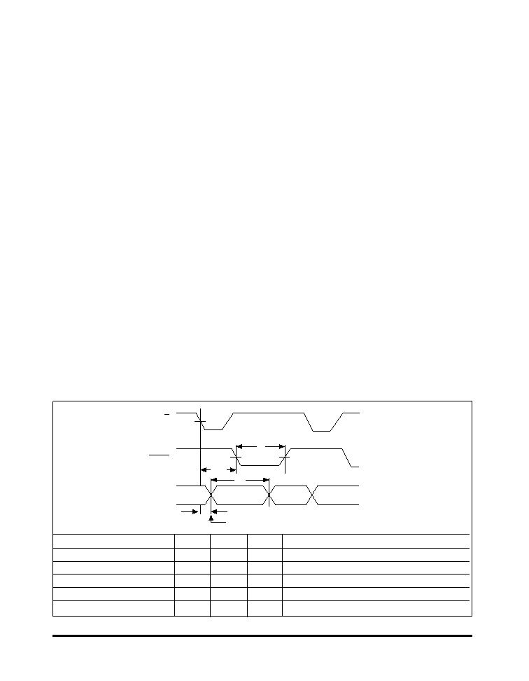
Figure 4. Acquisition and Conversion Timing
R/C
BUSY
Converter
Mode
Acquisition
Conversion
Acquisition
Conversion
tAP
Hold Time
t C
t DBC
tB
SYMBOL/PARAMETER
MIN
TYP
MAX
UNITS
t
DBC
BUSY delay from R/C
80
150
ns
t
B
BUSY Low
2.5
2.7
s
t
AP
Aperture Delay
13
ns
t
AP
Aperture Jitter
150
ps, rms
t
C
Conversion Time
2.47
2.70
s
相关PDF资料 |
PDF描述 |
|---|---|
| SP7802SQ/883 | 12-BIT SUCCESSIVE APPROXIMATION ADC, PARALLEL ACCESS, CDIP24 |
| SP809EK-L-2-3 | 1-CHANNEL POWER SUPPLY SUPPORT CKT, PDSO3 |
| SP810EK-2.3/TR | 1-CHANNEL POWER SUPPLY SUPPORT CKT, PDSO3 |
| SP8121BS | 8-CH 12-BIT SUCCESSIVE APPROXIMATION ADC, PARALLEL ACCESS, PDSO32 |
| SP813MCN-L | 1-CHANNEL POWER SUPPLY SUPPORT CKT, PDSO8 |
相关代理商/技术参数 |
参数描述 |
|---|---|
| SP7800AKN | 制造商:SIPEX 制造商全称:Sipex Corporation 功能描述:12-Bit 3ms Sampling A/D Converter |
| SP7800AKS | 制造商:SIPEX 制造商全称:Sipex Corporation 功能描述:12-Bit 3ms Sampling A/D Converter |
| SP7805AIS WAF | 制造商:Texas Instruments 功能描述: |
| SP7805V2-L | 功能描述:DC/DC 开关控制器 30 TERMINAL 1A POS RoHS:否 制造商:Texas Instruments 输入电压:6 V to 100 V 开关频率: 输出电压:1.215 V to 80 V 输出电流:3.5 A 输出端数量:1 最大工作温度:+ 125 C 安装风格: 封装 / 箱体:CPAK |
| SP7805V2-L/TR | 功能描述:DC/DC 开关控制器 30 TERMINAL 1A POS RoHS:否 制造商:Texas Instruments 输入电压:6 V to 100 V 开关频率: 输出电压:1.215 V to 80 V 输出电流:3.5 A 输出端数量:1 最大工作温度:+ 125 C 安装风格: 封装 / 箱体:CPAK |
发布紧急采购,3分钟左右您将得到回复。