- 您现在的位置:买卖IC网 > PDF目录374928 > SSD1815T2R (Electronic Theatre Controls, Inc.) SEMICONDUCTOR TECHNICAL DATA PDF资料下载
参数资料
| 型号: | SSD1815T2R |
| 厂商: | Electronic Theatre Controls, Inc. |
| 英文描述: | SEMICONDUCTOR TECHNICAL DATA |
| 中文描述: | 半导体技术数据 |
| 文件页数: | 12/35页 |
| 文件大小: | 856K |
| 代理商: | SSD1815T2R |
第1页第2页第3页第4页第5页第6页第7页第8页第9页第10页第11页当前第12页第13页第14页第15页第16页第17页第18页第19页第20页第21页第22页第23页第24页第25页第26页第27页第28页第29页第30页第31页第32页第33页第34页第35页
SSD1815
12
REV 1.5
03/2000
S OLOMON
Reset Circuit
This block includes Power On Reset circuitry and the Reset pin,
RES. Both of these having the same reset function. Once RES
receives a negative reset pulse, all internal circuitry will start to initial-
ize. Minimum pulse width for completing the reset sequence is 1us.
The status of the chip after reset is given by:
1.
Display is turned OFF
2.
132X64 Display Display Mode with seperated Icon Line
3.
Normal segment and display data column address mapping
(SEG0 mapped to address 00h)
4.
Read-modify-write mode is OFF
5.
Power control register is set to 000b
6.
Shift register data clear in serial interface
7.
Bias ratio is set to 1/9
8.
Static indicator is turned OFF
9.
Display start line is set to display RAM column address 0
10. Column address counter is set to 0
11. Page address is set to 0
12. Normal scan direction of the COM outputs
13. Contrast control register is set to 20h
14. Test mode is turned OFF
Display Data Latch
A series of registers carrying the display signal information. For
SSD1815, there are 197 latches (132 + 65) for holding the data,
which will be fed to the HV Buffer Cell and Level Selector to output
the required voltage level.
Level Selector
Level Selector is a control of the display synchronization. Display
voltage can be separated into two sets and used with different cycles.
Synchronization is important since it selects the required LCD voltage
level to the HV Buffer Cell, which in turn outputs the COM or SEG LCD
waveform.
HV Buffer Cell (Level Shifter)
HV Buffer Cell work as a level shifter which translates the low voltage
output signal to the required driving voltage. The output is shifted out
with an internal FRM clock which comes from the Display Timing Gen-
erator. The voltage levels are given by the level selector which is syn-
chronized with the internal M signal.
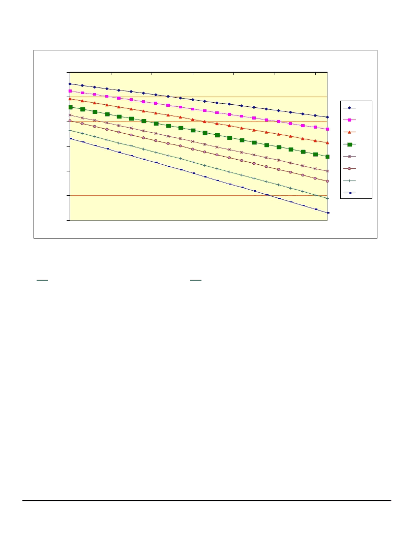
Figure 7 - Contrast Curves at Different Interneal Feedback Resistor Ratio Settings
VL6 vs Contrast Settings
-15
-13
-11
-9
-7
-5
-3
0
10
20
30
40
50
60
contrast level at VDD = 2.775V
V
20
21
22
23
24
25
26
27
相关PDF资料 |
PDF描述 |
|---|---|
| SSD1815T3R | SEMICONDUCTOR TECHNICAL DATA |
| SSD1815TR | SEMICONDUCTOR TECHNICAL DATA |
| SSD1815Z | SEMICONDUCTOR TECHNICAL DATA |
| SSD1818A | LCD Segment / Common Driver with Controller |
| SSD1818ATR1 | LCD Segment / Common Driver with Controller |
相关代理商/技术参数 |
参数描述 |
|---|---|
| SSD1815T3R | 制造商:未知厂家 制造商全称:未知厂家 功能描述:SEMICONDUCTOR TECHNICAL DATA |
| SSD1815TR | 制造商:未知厂家 制造商全称:未知厂家 功能描述:SEMICONDUCTOR TECHNICAL DATA |
| SSD1815Z | 制造商:未知厂家 制造商全称:未知厂家 功能描述:SEMICONDUCTOR TECHNICAL DATA |
| SSD1818 | 制造商:未知厂家 制造商全称:未知厂家 功能描述:LCD Segment / Common Driver with Controller |
| SSD1818A | 制造商:未知厂家 制造商全称:未知厂家 功能描述:LCD Segment / Common Driver with Controller |
发布紧急采购,3分钟左右您将得到回复。