- 您现在的位置:买卖IC网 > PDF目录374928 > SSD1815T2R (Electronic Theatre Controls, Inc.) SEMICONDUCTOR TECHNICAL DATA PDF资料下载
参数资料
| 型号: | SSD1815T2R |
| 厂商: | Electronic Theatre Controls, Inc. |
| 英文描述: | SEMICONDUCTOR TECHNICAL DATA |
| 中文描述: | 半导体技术数据 |
| 文件页数: | 6/35页 |
| 文件大小: | 856K |
| 代理商: | SSD1815T2R |
第1页第2页第3页第4页第5页当前第6页第7页第8页第9页第10页第11页第12页第13页第14页第15页第16页第17页第18页第19页第20页第21页第22页第23页第24页第25页第26页第27页第28页第29页第30页第31页第32页第33页第34页第35页
SSD1815
6
REV 1.5
03/2000
S OLOMON
MSTAT
This pin is the static indicator driving output. It is only active in
master operation. The frame signal output pin, M, should be used
as the back plane signal for the static indicator.
The duration of overlapping could be programmable. See
Extended Command Table for details.
This pin becomes high impedance if the chip is operating in
slave mode.
M
This pin is the frame signal input/output. In master mode, the pin
supplies frame signal to slave devices while in slave mode, the pin
receives frame signal from the master device.
CL
This pin is the display clock input/output. In master mode, the pin
supplies display clock signal to slave devices while in slave mode,
the pin receives display clock signal from the master device.
DOF
This pin is diaplay blanking control between master and slave
devices. In master mode, this pin supplies on/off signal to slave
devices. In slave mode, this pin receives on/off signal from the
master device.
CS1
,
CS2
These pins are the chip select inputs. The chip is enabled for
MCP communication only when both CS1 is pulled low and CS2 is
pulled high.
RES
This pin is reset signal input. Initialization of the chip is started
once this pin is pulled low. Minimum pulse width for completing the
reset is 1us.
D/C
This pin is Data/Command control pin. When the pin is pulled
high, the data at D
7
-D
0
is treated as display data. When the pin is
pulled low, the data at D
7
-D
0
will be tranferred to the command reg-
ister.
R/W(WR)
This pin is microprocessor interface input. When interfacing to an
6800-series microprocessor, this pin will be used as R/W singal
input. Read mode will be carried out when this pin is pulled high
and write mode when low.
When interfacing to an 8080-microprocessor, this pin will be the
WR input. Data write operation is initiated when this pin is pulled
low when the chip is selected.
E(RD)
This pin is microprocessor interface input. When interfacing to an
6800-series microprocessor, this pin will be used as the enable sig-
nal, E. Read/write operation is initiated when this pin is pulled high
when the chip is selected.
When interfacing to an 8080-microprocessor, this pin receives
the RD signal. Data read operation is initiated when this pin is
pulled low when the chip is selected.
D
7
-D
0
These pins are the 8-bit bi-directional data bus to be connected
to the microprocessor in parallel interface mode. D
7
is the MSB
while D
0
is the LSB.
When serial mode is selected, D
7
is the serial data input (SDA)
and D
6
is the serial clock input (SCK).
V
DD
Power supply pin.
V
SS
Ground.
V
SS1
Reference voltage input for internal DC-DC converter. The volt-
age of generated, V
EE
, equals to the multiple factor times the pro-
tential different between this pin, V
SS1
, and V
DD
. The multiple
factor, 2X, 3X or 4X, is selected by different external capacitor
connections. All voltage levels are referenced to V
DD
.
Note: the potential at this input pin must lower than or equal to
V
SS
.
V
EE
This is the most negative voltage supply pin of the chip. It can
be supplied externally or generated by the internal DC-DC con-
verter.
When using internal DC-DC converter as generator, voltage at
this pin is for internal reference only. It CANNOT be used for driv-
ing external circuitries.
C
3N
, C
1P
, C
1N
, C
2N
and C
2P
When internal DC-DC voltage converter is used, external
capacitor(s) is/are connected between these pins. Different con-
nection will result in different DC-DC converter multiple factor, 2X,
3X or 4X. Details please refer to voltage converter section in the
block diagram description.
V
FS
This is an input pin to provide an external voltage reference for
the internal voltage regulator. The function of this pin is only
enabled for the External Input chip models which are required
special ordering. For normal chip model, please leave this pin NC.
V
L2
, V
L3
, V
L4
and V
L5
(Voltages referenced to V
DD
)
LCD driving voltages. They can be supplied externally or gener-
ated by the internal bias divider. They have the following relation-
ship:
V
DD
> V
L2
> V
L3
> V
L4
> V
L5
> V
L6
V
L6
This pin is the most negative LCD driving voltage. It can be sup-
plied externally or generated by the internal regulator.
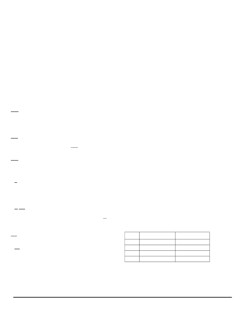
1:7 bias
1:9 bias (default)
V
L2
V
L3
V
L4
V
L5
1/7*V
L6
2/7*V
L6
5/7*V
L6
6/7*V
L6
1/9*V
L6
2/9*V
L6
7/9*V
L6
8/9*V
L6
PIN DESCRIPTIONS
相关PDF资料 |
PDF描述 |
|---|---|
| SSD1815T3R | SEMICONDUCTOR TECHNICAL DATA |
| SSD1815TR | SEMICONDUCTOR TECHNICAL DATA |
| SSD1815Z | SEMICONDUCTOR TECHNICAL DATA |
| SSD1818A | LCD Segment / Common Driver with Controller |
| SSD1818ATR1 | LCD Segment / Common Driver with Controller |
相关代理商/技术参数 |
参数描述 |
|---|---|
| SSD1815T3R | 制造商:未知厂家 制造商全称:未知厂家 功能描述:SEMICONDUCTOR TECHNICAL DATA |
| SSD1815TR | 制造商:未知厂家 制造商全称:未知厂家 功能描述:SEMICONDUCTOR TECHNICAL DATA |
| SSD1815Z | 制造商:未知厂家 制造商全称:未知厂家 功能描述:SEMICONDUCTOR TECHNICAL DATA |
| SSD1818 | 制造商:未知厂家 制造商全称:未知厂家 功能描述:LCD Segment / Common Driver with Controller |
| SSD1818A | 制造商:未知厂家 制造商全称:未知厂家 功能描述:LCD Segment / Common Driver with Controller |
发布紧急采购,3分钟左右您将得到回复。